


 The Chemical Connection: Reducing Etch System Water Usage, Part 2
 It’s Only Common Sense: Nice Guys Really Can Finish First
 The Right Approach: I Hear the Train A Comin'
Agile Analog Fast Tracks IoT Design with Macros for Analog Functions
October 21, 2022 | Agile AnalogEstimated reading time: 2 minutes
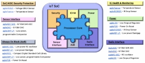
Agile Analog, the analog IP innovators, now has available a complete set of the key analog IP needed to fast track an IoT design. Arranged in six blocks, they wrap round the customer’s choice of processor core and memory to provide all the vital analog functions required to interface between the digital world of the processor and the analog real world.
Barry Paterson, Agile Analog’s CEO, explained, “We call these our Foundation IP as they provide all the functionality needed for an IoT design. Naturally, customers can mix and match whichever blocks they require for their design and adjust the number of each IP within it.”
For example, the Power block could contain several agileLDOs to provide the necessary internal voltage rails together with agilePOR to ensure the SoC only starts when stable voltage rails are present. The IC Heath and Monitoring block monitors the SoC die temperature with the agileTsense whilst the agileIR DROP monitors long term aging effects.
Ensuring the SoC is secure is a key concern today, so the Security Protection block uses the agileVGlitch and agileTsense to monitor attack vectors using voltage and temperature manipulation. Customers may not need a radio interface but, if they do, the Radio Interface can support whichever one they require, such as low power Bluetooth or LoRa.
“Effectively this provides a foundation toolkit for all the analog parts that a design might possibly need to fast track, simplify and re-risk the design process,” he added. “We have included all the features and functions that a customer would require so that they can select exactly what they require from the set without worrying that they missed something vital.
“Importantly, the high level of customer support that we provide ensures easy and perfect integration unlike some rivals who just sell the analog blocks and leave customers to figure out how to use them. Also, customers have the security of knowing that, by using IP from one supplier, all our IP blocks have been fully tested for compatibility with every other one of our blocks.”
A key feature of Agile Analog’s offering is that it is fully supported by the company for the design phase to ensure that it meets the Power, Performance and Area requirements of the design. This also includes supporting the integration of the IP into the overall design. This is made easier by the IPs within the blocks being internally interconnected and that the blocks have external interfaces so that they look like digital blocks and can drop into the digital design flow.
Agile Analog’s innovative Composa™ technology enables these blocks to be generated and validated for whatever process and node that the customer requires. It can rapidly regenerate a solution should this change enabling easy portability between foundries and processes. All the major foundries are supported including TSMC, GlobalFoundries, Samsung Foundry and SMIC as well as other IC foundries and manufacturers.
The six blocks are:
- SoC/ASIC Security Protection with voltage glitch sensor and temperature sensor.
- Sensor Interface with 8/10-bit SAR ADC, 8/10-bit DAC, and low power programmable comparator
- Always on Block with low power RC oscillator, low power bandgap, compact digital standard cell library, low power programmable comparator and power on rest.
- IC Health and Monitoring with temperature sensor and IR drop sensor.
- Power with low dropout regulator, power on reset, IR drop sensor and low power bandgap.
- Radio Interface with 8/10-bit SAR ADC, 8/10-bit DAC, RC oscillator and low dropout regulator.
Share on:


Suggested Items
Real Time with… IPC APEX EXPO 2024: Ventec Discusses New Pro-bond Family of Advanced Products
05/01/2024 | Real Time with...IPC APEX EXPOChris Hanson, Ventec's Global Head of IMS Technology, outlines the launch of four pro-bond formulas that deliver an outstanding combination of low dissipation factor (Df) with a dielectric constant (Dk) range to maximize the design window for critical PCB parameters. As Chris points out, Pro-bond is designed for low-loss, high-speed applications, while thermal-bond dissipates heat from a component through the board to a heat sink.
IPC's Vision for Empowering PCB Design Engineers
04/30/2024 | Robert Erickson, IPCAs architects of innovation, printed circuit board designers are tasked with translating increasingly complex concepts into tangible designs that power our modern world. IPC provides the necessary community, standards framework, and education to prepare these pioneers as they explore the boundaries of what’s possible, equipping engineers with the knowledge, skills, and resources required to thrive in an increasingly dynamic field.
On the Line With… Talks With Cadence Expert on SI/PI for PCB Designers
05/02/2024 | I-Connect007In “PCB 3.0: A New Design Methodology—SI/PI for PCB Designers,” subject matter expert Brad Griffin, Cadence Design Systems, discusses how an intelligent system design methodology can move some signal and power integrity decision-making into the physical design space, offering real-time feedback.
iNEMI Packaging Tech Topic Series: Role of EDA in Advanced Semiconductor Packaging
04/26/2024 | iNEMIAdvanced semiconductor packaging with heterogenous integration has made on-package integration of multiple chips a crucial part of finding alternatives to transistor scaling. Historically, EDA tools for front-end and back-end design have evolved separately; however, design complexity and the increased number of die-to-die or die-to-substrate interconnections has led to the need for EDA tools that can support integration of overall design planning, implementation, and system analysis in a single cockpit.
Cadence, TSMC Collaborate on Wide-Ranging Innovations to Transform System and Semiconductor Design
04/25/2024 | Cadence Design SystemsCadence Design Systems, Inc. and TSMC have extended their longstanding collaboration by announcing a broad range of innovative technology advancements to accelerate design, including developments ranging from 3D-IC and advanced process nodes to design IP and photonics.