


 It’s Only Common Sense: OCCAM—the Time Is Now
 Marcy's Musings: The Growing Industry
 Dan’s Biz Bookshelf: Seeing the How
High-Efficient Beam Sources for Highly Productive Electronics Production
December 15, 2016 | LPKFEstimated reading time: 1 minute
The role of laser technology in the manufacture of electronic components and products continues to grow. For instance, more than 20 different laser processes are used in the production of smartphones, such as for structuring thin layers, for producing three-dimensional conductor structures on plastic bodies, and for cutting glass and printed circuit boards.
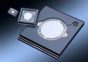
Hermetically sealed 2D MEMS scanners as an element of the InBUS project. (Source: Fraunhofer ISIT)
For these applications, the importance of short-pulse and ultrashort-pulse lasers is continually rising. The joint project “(U)SP Laser Beam Sources for Industrial Use and System-wide Productivity Improvement for Highly Dynamic Drilling and Cutting Applications” (InBUS) focuses on increasing efficiency, available output power, and flexibility of these laser sources.
New laser beam sources only constitute a portion of the necessary process technology - the manufacturing industry requires complete systems that are productive and efficient. In order to remain competitive and incorporate new applications, the capacity of the laser systems needs to be improved continuously. Two challenges arise in connection with development of laser beam sources:
- efficient guiding of the laser radiation to the workpiece,
- productive movement of the beam across the workpiece.
Therefore, further application-focused development of beam sources requires parallel development of beam guidance and beam deflection systems. This increases acceptance of laser technology in production and opens up new avenues for more cost-effective products with novel functions.
In the course of the public funded InBUS project, solutions for these two challenges will be developed in form of system-related solutions for selected applications, with emphasis on the structuring of electronic components - in particular, on drilling and cutting printed circuit boards.
The objective of the project is to devise highly efficient system technology adapted to specific applications by developing the most important components from scratch. LPKF is developing laser sources based on novel concepts for increasing energy efficiency and flexibility. Two different laser sources are used for demonstration of the pilot application.
A combination of conventional and novel scanning technology is employed as a solution for application-specific beam guidance. To this end, Qubig is developing new electro-optical deflectors (EOD), Fraunhofer ISIT focuses on micro-electromechanical mirrors (MEMS). In order to provide efficient beam delivery, Photonic Tools is refining its fiber technology. The combination of these technologies enables processing of large substrates at a high throughput rate. As an associated partner, Continental will be testing and evaluating de-veloped scanner solutions.
Share on:


Suggested Items
Real Time with… IPC APEX EXPO 2024: Plasmatreat: Innovative Surface Preparation Solutions
04/25/2024 | Real Time with...IPC APEX EXPOIn this interview, Editor Nolan Johnson speaks with Hardev Grewal, CEO and president of Plasmatreat, a developer of atmospheric plasma solutions. Plasmatreat uses clean compressed air and electricity to create plasma, offering environmentally friendly methosd for surface preparation. Their technology measures plasma density for process optimization and can remove organic micro-contamination. Nolan and Hardev also discuss REDOX-Tool, a new technology for removing metal oxides.
Nanotechnology Market to Surpass $53.51 Billion by 2031
04/25/2024 | PRNewswireSkyQuest projects that the nanotechnology market will attain a value of USD 53.51 billion by 2031, with a CAGR of 36.4% over the forecast period (2024-2031).
Cadence, TSMC Collaborate on Wide-Ranging Innovations to Transform System and Semiconductor Design
04/25/2024 | Cadence Design SystemsCadence Design Systems, Inc. and TSMC have extended their longstanding collaboration by announcing a broad range of innovative technology advancements to accelerate design, including developments ranging from 3D-IC and advanced process nodes to design IP and photonics.
SMC Korea 2024 to Highlight Semiconductor Materials Trends and Innovations on Industry’s Path to $1 Trillion
04/24/2024 | SEMIWith Korea a major consumer of semiconductor materials and advanced materials a key driver of innovation on the industry’s path to $1 trillion, industry leaders and experts will gather at SMC (Strategic Materials Conference) Korea 2024 on May 29 at the Suwon Convention Center in Gyeonggi-do, South Korea to provide insights into the latest materials developments and trends. Registration is open.
Orbex Secures £16.7m Investment for Rocket ‘Ramp Up’ Period
04/24/2024 | OrbexThe UK spaceflight company Orbex has received £16.7m from six backers in an update to its Series C funding round.