


 Marcy's Musings: The Growing Industry
 It’s Only Common Sense: Here’s What To Do After IPC APEX EXPO 2024
 Dan’s Biz Bookshelf: Seeing the How
AT&S to Present Latest Technologies and Products at Nepcon 2017
December 16, 2016 | AT&SEstimated reading time: 2 minutes
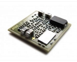
At Nepcon 2017 (18-20 January 2017) in Tokyo, AT&S will be presenting innovative technologies as a response to current challenges in telecommunication, automotive electronics, wearables and medical electronics. Advancing miniaturisation, high data rates and/or high frequencies, power electronics with increasing current densities and rising thermal problems, as well as optimised production processes are the challenges that modern applications face. AT&S will therefore present solutions for extremely compact substrates/modules, advanced heat management, Embedded Component Packaging (ECP®), HF printed circuit boards (PCBs) (such as automotive radar) and flexible PCBs for medical devices.
As part of their “Advanced Packaging”, AT&S have developed special process engineering solutions for component and semiconductor packaging – from embedding passive components to ECP for System-in-Boards (SiB) and System-in-Packages (SiP). The company now supplies ECP products in volume production, and has already implemented numerous products ranging from computer boards to medical sensor products and MEMS microphones.
Many applications demand ever higher power densities, while at the same time heat dissipation has to be optimised. AT&S offers an embedded technology with galvanic copper and silver sinter interconnections that enables highly efficient power packages with minimal thermal and electrical resistance. This technology’s performance will be on show with 50 and 500 W demonstrators (pedelec applications) using embedded MOSFETs, passive components and logic circuits. Extensive tests have proven the designs’ high thermal and shock performance as well as excellent switching behaviour.
Inadequate thermal management is a frequent cause of faults in electronic designs using modern power semiconductors such as MOSFETs, IGBTs or GTOs with ever higher switching frequencies and/or more compact modules. So the key issue is to dissipate the heat from critical components. One possibility, for example, is to integrate “heat pipes” into the PCB. Heat is then better distributed across the PCB as a whole. Another innovative solution is to implement graphite inlays, which have better thermal conductivity than copper by a factor of 2 to 5.
Ever higher speeds and HF designs also place high demands on printed circuit board technology. Technology drivers here include telecommunication on the path to 5G, but also the automotive industry with regard to automated/autonomous driving with complex driver assistance systems. The latter require numerous sensors, particularly radar at 24 to 77 GHz, and rapid processing of high data rates. On the materials side, AT&S is working intensively on products for the 35 to 90 GHz range with extremely low dielectric constants and loss factors. Other options for optimising transmission rates include the use of copper foils with reduced roughness, and process optimisations to reduce variations in the copper thickness. An efficient combination of logic and HF circuit enables the X-in-Board concept, in which, for example, a standard FR4 PCB is combined with a HF PCB. HF designs implemented by AT&S range from wireless 60 GHz communication products to 77 GHz radar systems for automobiles.
AT&S has also obtained certification for medical devices under the EN ISO 13485 standard. These diverse applications include diagnostic instruments (MRI, X-ray, ultrasound, etc.) but also therapeutic devices such as defibrillators, pacemakers and hearing aids, as well as blood glucose meters and ECGs. Surgical tools, biochips and RFID applications benefit from AT&S technologies too, such as flexible and rigid-flexible PCBs.
AT&S will be presenting its latest technologies and products at Nepcon 2017 – Asia’s leading exhibition for electronics development and manufacturing – in Tokyo from 18-20 January.
Share on:


Suggested Items
IPC Bestows Posthumous Hall of Fame Award to Industry Icon Michael Ford
04/18/2024 | IPCIPC honored the late Michael Ford, Aegis Software, for his extraordinary contributions to the global electronics manufacturing industry with the IPC Raymond E. Pritchard Hall of Fame Award at IPC APEX EXPO 2024. IPC’s most prestigious honor, the Hall of Fame Award is given to individuals who have provided exceptional service and advancement to IPC and the electronics industry. Ford, an industry leader and valued IPC volunteer, died suddenly in January 2024.
SEMI Applauds U.S. Chips Act Award for Samsung Electronics Facilities to Strengthen Domestic Semiconductor Supply Chain
04/17/2024 | SEMISEMI, the industry association serving the global electronics design and manufacturing supply chain, applauded the United States Department of Commerce’s announcement of a Preliminary Memorandum of Terms for an award under the CHIPS and Science Act to support the expansion of Samsung Electronics’ presence in Texas and the company’s development and production of leading-edge chips.
Northrop Grumman honors Calumet Electronics with Supplier Excellence Award
04/17/2024 | Calumet ElectronicsNorthrop Grumman Corporation has recognized Calumet Electronics during the company’s 2024 Supplier Excellence Awards for “exceptional performance and unwavering commitment to delivering with excellence.” Calumet is one of 70 suppliers recognized from across the globe. In its award category of “Supplier Strategic Excellence,” Calumet was honored alongside global corporations such as Amazon Web Services, Dell Technologies, and Eaton Corporation.
Ark Electronics Expands Global Manufacturing Factory Network in North America and Europe
04/17/2024 | PRNewswireElectronic Manufacturing Company Ark Electronics recently announced the expansion of its Global Factory Network with the addition of Electronics Manufacturing Service (EMS) capabilities in Mexico and Europe.
Designing Electronics for High Thermal Loads
04/16/2024 | Akber Roy, Rush PCB Inc.Developing proactive thermal management strategies is important in the early stages of the PCB design cycle to minimize costly redesign iterations. Here, I delve into key aspects of electronic design that hold particular relevance for managing heat in electronic systems. Each of these considerations plays a pivotal role in enhancing the reliability and performance of the overall system.