


 Marcy's Musings: The Growing Industry
 It’s Only Common Sense: Here’s What To Do After IPC APEX EXPO 2024
 Dan’s Biz Bookshelf: Seeing the How
SelectConnect Technologies Publishes White Paper on Laser Direct Structuring
April 5, 2017 | SelectConnect TechnologiesEstimated reading time: 1 minute
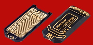
SelectConnect Technologies has published the white paper, “Trace Width and Space Limitations for Laser Direct Structuring.” The white paper details a study that was conducted to determine how close laser direct structuring (LDS) traces can be created and metallized without inducing over plating or bridging on PET/PBT material.
A geometric pattern with varying trace widths and spacing distances were structured onto plaques made from the three different materials. The plaques were subsequently plated with copper, nickel, and immersion gold and examined for signs of over plating. Trace widths and spacing were measured using video microscopy equipment.
Laser direct structuring (LDS) is the first step of a manufacturing process that creates circuit traces on three-dimensional molded thermoplastic components. Currently the leading technology for producing cell phone antennas, LDS has also been widely employed to manufacture a range of components for use in medical devices, security shields, automotive sensors, and GPS antennas-- anywhere product miniaturization requires embedding circuits onto a molded component of a device.
About SelectConnect Technologies
SelectConnect Technologies specializes in the production of three-dimensional molded interconnect devices (3D-MID), offering both laser direct structuring (LDS) and 2-shot injection capabilities. Working with LPKF since 2010, the company has produced thousands of laser direct structured components for a wide range of applications. With expertise in electroless metallization, SelectConnect also produces molded interconnect device plating to construct circuitry with the comparable function and performance of a printed circuit board.
To read and download the white paper, please click here or email solutions@selectconnettech.com.
Share on:


Suggested Items
Insulectro’s 'Storekeepers' Extend Their Welcome to Technology Village at IPC APEX EXPO
04/03/2024 | InsulectroInsulectro, the largest distributor of materials for use in the manufacture of PCBs and printed electronics, welcomes attendees to its TECHNOLOGY VILLAGE during this year’s IPC APEX EXPO at the Anaheim Convention Center, April 9-11, 2024.
ENNOVI Introduces a New Flexible Circuit Production Process for Low Voltage Connectivity in EV Battery Cell Contacting Systems
04/03/2024 | PRNewswireENNOVI, a mobility electrification solutions partner, introduces a more advanced and sustainable way of producing flexible circuits for low voltage signals in electric vehicle (EV) battery cell contacting systems.
Heavy Copper PCBs: Bridging the Gap Between Design and Fabrication, Part 1
04/01/2024 | Yash Sutariya, Saturn Electronics ServicesThey call me Sparky. This is due to my talent for getting shocked by a variety of voltages and because I cannot seem to keep my hands out of power control cabinets. While I do not have the time to throw the knife switch to the off position, that doesn’t stop me from sticking screwdrivers into the fuse boxes. In all honesty, I’m lucky to be alive. Fortunately, I also have a talent for building high-voltage heavy copper circuit boards. Since this is where I spend most of my time, I can guide you through some potential design for manufacturability (DFM) hazards you may encounter with heavy copper design.
Trouble in Your Tank: Supporting IC Substrates and Advanced Packaging, Part 5
03/19/2024 | Michael Carano -- Column: Trouble in Your TankDirect metallization systems based on conductive graphite or carbon dispersion are quickly gaining acceptance worldwide. Indeed, the environmental and productivity gains one can achieve with these processes are outstanding. In today’s highly competitive and litigious environment, direct metallization reduces costs associated with compliance, waste treatment, and legal issues related to chemical exposure. What makes these processes leaders in the direct metallization space?
AT&S Shines with Purest Copper on World Recycling Day
03/18/2024 | AT&SThe Styrian microelectronics specialist AT&S is taking World Recycling Day as an opportunity to review the progress that has been made in recent months at its sites around the world in terms of the efficient use of resources: