


 It’s Only Common Sense: OCCAM—the Time Is Now
 Marcy's Musings: The Growing Industry
 Dan’s Biz Bookshelf: Seeing the How
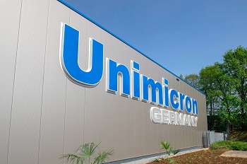
Unimicron Germany Rises from the Ashes with New Smart Factory
April 30, 2018 | Pete Starkey, I-Connect007 and Michael Weinhold, EIPCEstimated reading time: 9 minutes
This is a review of the grand opening of Unimicron’s new smart factory in Geldern, Germany.
A fire in a PCB shop is an experience we all dread, but still it happens, and the consequences can be devastating. In the early hours of December 28, 2016, the innerlayer production plant at RUWEL International in Geldern, Germany, caught fire and the whole factory and its contents were destroyed.
Figure 1: Aerial photo of the burned-out factory. (Source: EIPC)
Thankfully, there were no casualties and because the chemical stores survived, there were no serious environmental consequences. However, early estimates of the cost of the damage ran into higher-double-digit millions of Euros. And to quote the words of CTO Rico Schlüter “...we have unfortunately not the time to mourn—we must tackle today's challenges and come back as an even stronger company."
Recognised as the oldest operating PCB producer in Europe, RUWEL International GmbH was founded in Geldern in 1945. Unimicron Group made a strategic investment in RUWEL in 2009, and in 2011 fully integrated the company into the group, developing it as the leader of their High Reliability Business Unit (HRBU). More recently, the operation has been re-named Unimicron Germany. The parent organisation, headquartered in Taiwan, is the global leader in the PCB industry, with an annual turnover of $2 billion, 14 Asian production facilities, and a workforce of over 20,000.
Meanwhile, in Geldern, the pressure was on to move fast to maintain continuity of supply to RUWEL’s customer base. Only a few hours after the fire, and in consultation with Unimicron, it was decided that a new innerlayer production facility should be built in Geldern, with the production needs supported with mass-lam from the Unimicron plant in Kunshan, China—already qualified and certified with the approvals required by RUWEL’s automotive market.
I have always been encouraged by the community spirit which exists in our industry, especially when misfortune strikes. On several occasions over many years of personal experience I have seen how suppliers, friends and even competitors rally round to offer practical help, and this was very much the case for RUWEL who were able to benefit from local resources to support small batch and quick-turn requirements in the interim period, all with the approval and cooperation of their customers.
In the meantime, the company was re-named Unimicron Germany.
So, with continuity of production secured, planning of the replacement factory went ahead and in August 2017 the City of Geldern gave Unimicron formal permission for the rebuilding work to commence. Orders were placed for equipment that would represent the state of the art both in technology and in smart factory automation.
It all became a reality on Saturday 21st April 2018, when together with suppliers, customers, the Unimicron workforce and the officers of the EIPC, I was one of 800 guests privileged to attend the opening ceremony and to have a guided tour of the new facility—a spectacular experience!
Although most visitors were being escorted in large groups around the factory with German-speaking guides, my EIPC colleagues and I had the benefit of a more exclusive, small-group walk-around in the company of CTO Rico Schlüter who had been instrumental in designing, installing and commissioning the whole set-up.
After congregating outside in hot sunshine, it was refreshing to feel the air conditioning as we entered the plant. First impression was white—white floor, white walls, white ceiling, fully-enclosed white equipment, lots of space, all the services out of sight, no clutter of racks or trolleys to be seen.
And we were greeted by a robot—an autonomous guided vehicle (AGV) carrying a sign welcoming us to Unimicron’s smart factory. It was yellow, as were its eight colleagues around the factory area, each robot AGV capable of performing any panel-transportation task in any area. No fear of getting run-over—these laser- and GPS-guided robots could identify humans and stop, even if someone suddenly stepped into their path, although they did tend to bleep rather impatiently if they had work to do and you happened to be standing in their way!
Figure 2: Welcoming robot AGV.
Automation was everywhere, with traceability to match; every panel in the factory had its own unique data-matrix ID. Whether the job was a quick-turn prototype or a series production batch, the required material was drawn from store by an automated picking system and transferred to an AGV, which transported it to the load station of one of three surface-preparation lines, from which it was fed by a six-axis robot onto the machine conveyor. The predominant panel size was 24” x 21” although 24” x 18” and 24” x 24” were alternative options.
Figure 3: Surface preparation line.
Figure 4: Rear of surface preparation line.
Figure 5: Six-axis robot loader.
Page 1 of 6
Share on:


Suggested Items
Designer’s Notebook: What Designers Need to Know About Manufacturing, Part 2
04/24/2024 | Vern Solberg -- Column: Designer's NotebookThe printed circuit board (PCB) is the primary base element for providing the interconnect platform for mounting and electrically joining electronic components. When assessing PCB design complexity, first consider the component area and board area ratio. If the surface area for the component interface is restricted, it may justify adopting multilayer or multilayer sequential buildup (SBU) PCB fabrication to enable a more efficient sub-surface circuit interconnect.
Insulectro’s 'Storekeepers' Extend Their Welcome to Technology Village at IPC APEX EXPO
04/03/2024 | InsulectroInsulectro, the largest distributor of materials for use in the manufacture of PCBs and printed electronics, welcomes attendees to its TECHNOLOGY VILLAGE during this year’s IPC APEX EXPO at the Anaheim Convention Center, April 9-11, 2024.
ENNOVI Introduces a New Flexible Circuit Production Process for Low Voltage Connectivity in EV Battery Cell Contacting Systems
04/03/2024 | PRNewswireENNOVI, a mobility electrification solutions partner, introduces a more advanced and sustainable way of producing flexible circuits for low voltage signals in electric vehicle (EV) battery cell contacting systems.
Heavy Copper PCBs: Bridging the Gap Between Design and Fabrication, Part 1
04/01/2024 | Yash Sutariya, Saturn Electronics ServicesThey call me Sparky. This is due to my talent for getting shocked by a variety of voltages and because I cannot seem to keep my hands out of power control cabinets. While I do not have the time to throw the knife switch to the off position, that doesn’t stop me from sticking screwdrivers into the fuse boxes. In all honesty, I’m lucky to be alive. Fortunately, I also have a talent for building high-voltage heavy copper circuit boards. Since this is where I spend most of my time, I can guide you through some potential design for manufacturability (DFM) hazards you may encounter with heavy copper design.
Trouble in Your Tank: Supporting IC Substrates and Advanced Packaging, Part 5
03/19/2024 | Michael Carano -- Column: Trouble in Your TankDirect metallization systems based on conductive graphite or carbon dispersion are quickly gaining acceptance worldwide. Indeed, the environmental and productivity gains one can achieve with these processes are outstanding. In today’s highly competitive and litigious environment, direct metallization reduces costs associated with compliance, waste treatment, and legal issues related to chemical exposure. What makes these processes leaders in the direct metallization space?