-

- News
- Books
Featured Books
- pcb007 Magazine
Latest Issues
Current Issue
The Growing Industry
In this issue of PCB007 Magazine, we talk with leading economic experts, advocacy specialists in Washington, D.C., and PCB company leadership to get a well-rounded picture of what’s happening in the industry today. Don’t miss it.
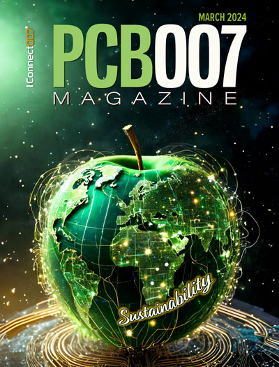
The Sustainability Issue
Sustainability is one of the most widely used terms in business today, especially for electronics and manufacturing but what does it mean to you? We explore the environmental, business, and economic impacts.
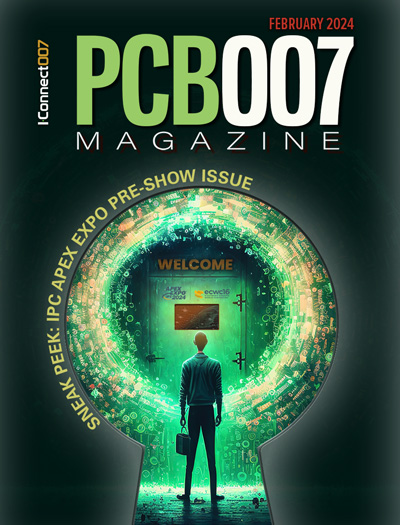
The Fabricator’s Guide to IPC APEX EXPO
This issue previews many of the important events taking place at this year's show and highlights some changes and opportunities. So, buckle up. We are counting down to IPC APEX EXPO 2024.
- Articles
Article Highlights
- Columns
Search Console
- Links
- Events
||| MENU - pcb007 Magazine
EIPC 50th Anniversary Conference Day 1: The Past, the Present and the Future, Pt. 1
July 13, 2018 | Pete Starkey, I-Connect007Estimated reading time: 16 minutes
Just like old times—meeting with John Ling, with whom I had previously travelled to industry events for over two decades, and who still carries the role of EIPC marketing manager, to fly together from Birmingham UK to Dusseldorf in Germany for the EIPC 50th Anniversary Summer Conference.
To borrow from Ling’s words of introduction in EIPC’s invitation to attend: “Half a century has passed since EIPC was founded in the days when the PCB was more than just a commodity. PCBs were technological works of art, and fellow artists came together to compare notes and to see which galleries were having good exhibitions and commissions.” And about the bonus-programme factory visit, the art gallery analogy continued as he described Unimicron's new multilayer facility in Geldern as “The Tate Modern of the European PCB industry.”
Representing 17 countries, 135 delegates were made welcome by EIPC President Alun Morgan, recently re-elected for a third term of office. He quoted Bernard Bismuth, long-time stalwart of the French industry, 43 years general manager of CCI Eurolam and currently Affiliate Professor at HEC in Paris, who described the PCB as: “The last product to be defined and the first to be needed, and it keeps changing!”
Morgan wound back the clock to 1968, the year in which EIPC was founded by Dr Mario Fassini, when Apollo 8 became the first manned spacecraft to orbit the Moon and return safely to Earth, Martin Luther King and Bobby Kennedy were assassinated, and a 3-kilometre geodesic dome covering Midtown Manhattan was proposed by Buckminster Fuller.
The form of Fuller’s geodesic dome was significant in the naming of spherical allotropes of carbon consisting of 60 atoms and 90 covalent bonds arranged in 12 hexagons and 20 pentagons— “Fullerene,” alternatively “Buckyballs.” Morgan challenged the audience to build a ball-and-stick molecular model of Fullerene and was impressed when Emma Hudson promptly presented him with a perfect replica!
The thread of his discussion progressed through carbon nano-tubes to the wonder-material graphene—even demonstrating how he made some of his own using a stick of graphite and a roll of adhesive tape—which he believed would be a key enabler in next-generation electronics.
Morgan concluded his introduction with greetings from founder Dr. Fassini, who had managed the institute through its first 25 years, and introduced Walt Custer, whose “business outlook on the global electronics industry with an emphasis on Europe” is always eagerly awaited and has deservedly become recognised as the definitive guide to what to expect in forthcoming months.
Custer began with words of warning: “I’m a little more subdued than I was last year. Leading indicators are starting to cool, and growth is slowing. Be aware that things could slow down.” His summary of business conditions in the world electronics industry indicated that after strong growth in 2017, expansion had now slowed, although the calculations could be significantly distorted by differences in exchange rates—apparent growth calculated in U.S. dollars far exceeded the figure based on Euros. Passive component shortages remained a big problem and memory demand continued to drive semiconductor sales. And, inevitably, these demands and shortages supported price increases. The principal growth drivers were automotive, industrial and Internet of Things, and 5G and other disruptive technologies were emerging. But geopolitical concerns remained very significant, and if trade disputes escalated there was a real risk of a global slowdown.
Custer foresaw major disruption in the automotive industry globally over the coming decade, with the trend towards autonomous vehicles initiating the restructuring of entire industry segments. And although many new jobs would be created, particularly in semiconductors and electronic systems, hundreds of thousands of existing ones could be lost.
Looking at the prospects for the European PCB industry, which represented less than 4% of world production, the total for 2017 had been estimated between 1.86 and 1.88 billion euro, split Germany 43%, Austria/Switzerland 18%, Italy 10%, France 9%, UK 8% and Scandinavia 2%. Top five European manufacturers were AT&S in Austria, Würth, Schweizer and KSG in Germany, and Elvia in France. Although continued growth was expected in 2018, it would not be as strong as in 2017, and uncertainty about the future of multinational treaties and trade agreements was having an adverse effect on business confidence.
Emilie Jolivet, Semiconductor and Software division director at Yole Développement, the "More than Moore" market research and strategy consulting company, was the second keynote presenter, with a discussion of developments in advanced substrates and embedded die technology that could lead to a renewal of the PCB industry. She commented that form factor was currently the main driver for PCBs and substrates. There was a technology gap between substrate manufacture, with lines and spaces at 5 microns trending to 2 microns, and PCB manufacture, with lines and spaces at 30 microns. The substrate-like-PCB (SLP) bridged this technology gap, although it needed investment in new manufacturing technologies to make it available and affordable.
With the demand for higher battery capacity in smartphones, the space available to accommodate the electronics continued to decrease, so circuit boards needed to be smaller and with more functionality. HDI was being pushed to its limits of interconnection density, and Apple had set a new trend by introducing SLP into its latest iPhones. SLP could effectively offer double the efficiency of HDI. For example, whereas a current smartphone might have a 10-layer HDI board with 40-micron line and space, the next generation could have 20-layer stacked SLP with 25-micron line and space and occupy 40% less space. PCB and substrate manufacturers had started producing SLP and investing in mSAP and a few already had the capability. It was forecast that by 2023, 17% of all smartphones would use SLP.
Jolivet spoke at length about embedded die packaging trends and cost considerations, and about embedded interconnections in substrate, with reference to Intel’s embedded multi-die interconnect bridge—a package without through-silicon-vias as an alternative to the costly 2.5D silicon interposer, with an embedded interposer in a flip-chip BGA substrate. Forecasts for embedded die revenues showed substantial growth not only in smartphones but in automotive power converter applications as well, for reasons of form factor, higher component integration with shorter interconnections, thermal management and protection from harsh environments.
Continuous improvements in manufacturing capability and yield enabled the embedding of higher value components. Embedded die packaging already offered solutions for low to middle power applications and the gap in integrated packaging for middle and high-power applications could be filled by embedding the die in the PCB.
Substrate manufacturers were trying to find their way into the packaging business, and many commercial and development partnerships had already been established in the supply chain. And China was entering a technology area which had been seen traditionally as European and Japanese.
Page 1 of 3
Suggested Items
AIM Solder’s Dillon Zhu to Present on Ultraminiature Soldering at SMTA China East
04/22/2024 | AIMAIM Solder, a leading global manufacturer of solder assembly materials for the electronics industry, is pleased to announce that Dillon Zhu will present on the topic: Ultraminiature Soldering: Techniques, Technologies, and Standards at SMTA China East. This event is being held at the Shanghai World Expo Exhibition & Convention Center from April 24-25.
AIM to Highlight NC259FPA Ultrafine No Clean Solder Paste at SMTA Wisconsin Expo & Tech Forum
04/18/2024 | AIMAIM Solder, a leading global manufacturer of solder assembly materials for the electronics industry, is pleased to announce its participation in the upcoming SMTA Wisconsin Expo & Tech Forum taking place on May 7 at the Four Points by Sheraton | Milwaukee Airport, in Milwaukee, Wisconsin.
Hentec/RPS Publishes an Essential Guide to Selective Soldering Processing Tech Paper
04/17/2024 | Hentec Industries/RPS AutomationHentec Industries/RPS Automation, a leading manufacturer of selective soldering, lead tinning and solderability test equipment, announces that it has published a technical paper describing the critical process parameters that need to be optimized to ensure optimal results and guarantee the utmost in end-product quality.
Empowering Electronics Assembly: Introducing ALPHA Innolot MXE Alloy
04/16/2024 | MacDermid Alpha Electronics SolutionsIn the rapidly evolving electronics industry, where innovation drives progress, MacDermid Alpha Electronics Solutions is committed to setting a new standard. Today, we are pleased to introduce ALPHA Innolot MXE, a revolutionary alloy meticulously engineered to address the critical needs of enhanced reliability and performance in modern electronic assemblies.
New Book on Low-temperature Soldering Now Available
04/17/2024 | I-Connect007I-Connect007 is pleased to announce that The Printed Circuit Assembler’s Guide to… Low-temperature Soldering, Vol. 2, by subject matter experts at MacDermid Alpha Electronics Solutions, is now available for download.
