-

- News
- Books
Featured Books
- pcb007 Magazine
Latest Issues
Current Issue
The Growing Industry
In this issue of PCB007 Magazine, we talk with leading economic experts, advocacy specialists in Washington, D.C., and PCB company leadership to get a well-rounded picture of what’s happening in the industry today. Don’t miss it.
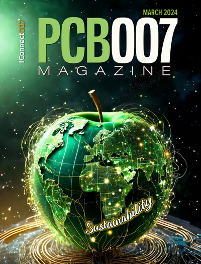
The Sustainability Issue
Sustainability is one of the most widely used terms in business today, especially for electronics and manufacturing but what does it mean to you? We explore the environmental, business, and economic impacts.
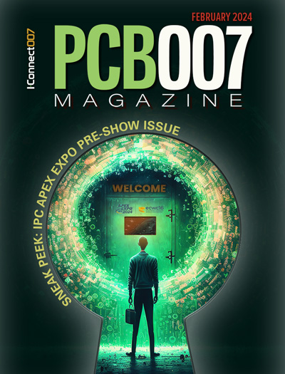
The Fabricator’s Guide to IPC APEX EXPO
This issue previews many of the important events taking place at this year's show and highlights some changes and opportunities. So, buckle up. We are counting down to IPC APEX EXPO 2024.
- Articles
- Columns
Search Console
- Links
- Events
||| MENU - pcb007 Magazine
Atotech to Discuss Reducing Manufacturing Costs for FO-PLP at iMAPS
October 8, 2018 | AtotechEstimated reading time: 2 minutes
“Upscaling panel size for copper plating on FO-PLP applications to reduce manufacturing cost” will be the topic of Atotech’s presentation at this year’s iMAPS conference, held in Pasadena, USA, from October 8 to 11, 2018.
Atotech’s presentation is part of Session TP2 on advanced fan-out and will be held by Christian Ohde, Global Application Manager for Panel and Pattern Plating and Dirk Ruess, Sales Development Manager for Electronics Equipment, on Tuesday, October 9, 2018, from 2:00-2:25 p.m.
“Since the successful implementation of Fan-Out Wafer-Level Packaging (FO-WLP) in the production of the iPhone 7 the industry is interested to increase the through-put and lower the total cost of ownership by moving from round wafer to panel format,” explains Christian Ohde. He continues “with Atotech’s MultiPlate®, a revolutionary new plating tool, the plating requirements for both wafer- and panel level packaging are met.”
The presentation will discuss the developments in FO-PLP and explain the current capability for copper distribution over panels for various panel formats (370 x 470 mm² up to 600 x 600 mm²). It will also introduce Atotech’s newly developed electrolytes for high-speed copper deposition in RDL plating - both with and without microvias and tall pillar plating (PoP design).
“Recently obtained process results show that FO-PLP has the potential to be not only a strong competition approach to FO-WLP, but seriously challenge the status quo in the coming years. High speed copper deposition enabled by the combination of new electrolytes and adapted plating equipment technology will be the answer of the challenges the industry currently faces,” adds Dirk.
MultiPlate PLP, Atotech’s revolutionary new tool for FO-PLP
The company will also present two topics at the poster session in the foyer on Thursday, October 11, from 11:45 a.m. to 1:15 p.m.:
- “Novel formaldehyde-free electroless copper for plating on next generation substrates” in poster session 140 by Christian Wendeln, R&D Scientist for Desmear and Metallization at Atotech Group
- “Investigation of a proactive glass filler removal in IC substrate build-up films and its effect on topography and copper adhesion” in poster session 146 by Stefan Kempa, R&D Scientist for Desmear and Metallization at Atotech Group
Atotech invites all iMAPS conference visitors to stop by and join their presentations on October 9 and 11. The Atotech team is also looking forward to discuss any other themes, trends and recent developments.
About Atotech
Atotech is one of the world’s leading manufacturers of specialty chemicals and equipment for the printed circuit board, IC-substrate and semiconductor industries, as well as for the decorative and functional surface finishing industries. Atotech has annual sales of USD1.2 billion (2017). The company is fully committed to sustainability – we develop technologies to minimize waste and to reduce environmental impact. Atotech has its headquarters in Berlin, Germany, and employs about 4,000 people in over 40 countries. For more information, click here.
Suggested Items
Insulectro’s 'Storekeepers' Extend Their Welcome to Technology Village at IPC APEX EXPO
04/03/2024 | InsulectroInsulectro, the largest distributor of materials for use in the manufacture of PCBs and printed electronics, welcomes attendees to its TECHNOLOGY VILLAGE during this year’s IPC APEX EXPO at the Anaheim Convention Center, April 9-11, 2024.
ENNOVI Introduces a New Flexible Circuit Production Process for Low Voltage Connectivity in EV Battery Cell Contacting Systems
04/03/2024 | PRNewswireENNOVI, a mobility electrification solutions partner, introduces a more advanced and sustainable way of producing flexible circuits for low voltage signals in electric vehicle (EV) battery cell contacting systems.
Heavy Copper PCBs: Bridging the Gap Between Design and Fabrication, Part 1
04/01/2024 | Yash Sutariya, Saturn Electronics ServicesThey call me Sparky. This is due to my talent for getting shocked by a variety of voltages and because I cannot seem to keep my hands out of power control cabinets. While I do not have the time to throw the knife switch to the off position, that doesn’t stop me from sticking screwdrivers into the fuse boxes. In all honesty, I’m lucky to be alive. Fortunately, I also have a talent for building high-voltage heavy copper circuit boards. Since this is where I spend most of my time, I can guide you through some potential design for manufacturability (DFM) hazards you may encounter with heavy copper design.
Trouble in Your Tank: Supporting IC Substrates and Advanced Packaging, Part 5
03/19/2024 | Michael Carano -- Column: Trouble in Your TankDirect metallization systems based on conductive graphite or carbon dispersion are quickly gaining acceptance worldwide. Indeed, the environmental and productivity gains one can achieve with these processes are outstanding. In today’s highly competitive and litigious environment, direct metallization reduces costs associated with compliance, waste treatment, and legal issues related to chemical exposure. What makes these processes leaders in the direct metallization space?
AT&S Shines with Purest Copper on World Recycling Day
03/18/2024 | AT&SThe Styrian microelectronics specialist AT&S is taking World Recycling Day as an opportunity to review the progress that has been made in recent months at its sites around the world in terms of the efficient use of resources:
