


 Marcy's Musings: The Growing Industry
 It’s Only Common Sense: Here’s What To Do After IPC APEX EXPO 2024
 Dan’s Biz Bookshelf: Seeing the How
Atotech Experts to Present at SEMICON Europa and electronica 2018
November 9, 2018 | AtotechEstimated reading time: 2 minutes
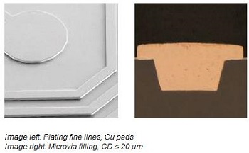
Atotech Group will exhibit and present its latest products for power, automotive, and mobile semiconductor applications at this year’s SEMICON Europa. Atotech’s Semiconductor portfolio includes RDL and pillar plating solutions for next generation FOWLP and 5G applications as well as solutions for electroless pad metallization and double side plating for power semiconductors.
SEMICON Europa is the largest and most influential gathering for the semiconductor industry in Europe and attracts more thought leaders from overseas every year. This year the SEMICON show will be co-located with electronica, an equivalently important show for the printed circuit board and electronics assembly industry. Both events take place in Munich, Germany, from November 13 to 16, 2018. While hall A4 will be dedicated to SEMICON Europa, hall B5 will feature electronica.
Atotech’s product experts will be present at booth 569 in hall A4 to discuss latest technology, trends, and future requirements. This year’s product features include:
- Spherolyte Cu UF3 - High purity ECD copper process for fine line RDL plating and microvia filling capability
- Spherolyte Cu VR - Electrochemical copper process for fine line plating and simultaneous filling of various via dimensions
- Xenolyte Ni TR - A high-temperature resistant electroless nickel process for RDL and pad metallization
- Spherolyte Cu MD2 and MultiPlate - A new low stress ECD copper process for power semiconductors that is developed to run in Atotech's next generation semiconductor plating tool: MultiPlate
Atotech experts will also participate in the adjacent program with several presentations:
- On Tuesday, November 13, at 4:40 pm, Ulrich Memmert, Senior Scientist Material Sciences, will talk about “Mechanical properties of copper for advanced packaging” at the Strategic Materials Conference in Room 14a
- On Wednesday, November 14, at 12:55 p.m., Ralf Schmidt, R&D manager semiconductor, will introduce the audience to the “Enhanced mechanical properties of copper for Fan Out Wafer Level Packaging applications” at the Advanced Packaging Conference in Room 13b
- On Thursday, November 15, at 10:45 a.m., Markus Hoerburger, Global Product Manager Semiconductor & Functional Electronics Coatings, will talk about “Optimized Cu plating solution for next generation packaging" at the TechLounge on the Showfloor show floor in Hall A4
- Also on Thursday, November 15, at 4:35 p.m., Andreas Walter, Team Manager Semiconductor Electroless Processes, will discuss “Electroless ternary nickel alloys for under bump metallization (UBM) on power semiconductors for high temperature process conditions or applications” at the TechArena 2, hall A4
- As part of the adjacent electronica, Roger Massey, technical marketing manager, will present “Recent developments in advanced HDI PCBs” at the “PCB & Components marketplace” in Hall A1 on Friday, November 16, at 10:00 a.m..
Visitors to the show are invited to attend Atotech’s presentations and stop by at booth 569 in Hall A4 to discuss and elaborate on these and other topics and trends driving the industry.
About Atotech
Atotech is one of the world’s leading manufacturers of specialty chemicals and equipment for the printed circuit board, IC-substrate and semiconductor industries, as well as for the decorative and functional surface finishing industries. Atotech has annual sales of $1.2 billion (2017). The company is fully committed to sustainability – we develop technologies to minimize waste and to reduce environmental impact. Atotech has its headquarters in Berlin, Germany, and employs about 4,000 people in over 40 countries. For more information, click here.
Share on:


Suggested Items
Insulectro’s 'Storekeepers' Extend Their Welcome to Technology Village at IPC APEX EXPO
04/03/2024 | InsulectroInsulectro, the largest distributor of materials for use in the manufacture of PCBs and printed electronics, welcomes attendees to its TECHNOLOGY VILLAGE during this year’s IPC APEX EXPO at the Anaheim Convention Center, April 9-11, 2024.
ENNOVI Introduces a New Flexible Circuit Production Process for Low Voltage Connectivity in EV Battery Cell Contacting Systems
04/03/2024 | PRNewswireENNOVI, a mobility electrification solutions partner, introduces a more advanced and sustainable way of producing flexible circuits for low voltage signals in electric vehicle (EV) battery cell contacting systems.
Heavy Copper PCBs: Bridging the Gap Between Design and Fabrication, Part 1
04/01/2024 | Yash Sutariya, Saturn Electronics ServicesThey call me Sparky. This is due to my talent for getting shocked by a variety of voltages and because I cannot seem to keep my hands out of power control cabinets. While I do not have the time to throw the knife switch to the off position, that doesn’t stop me from sticking screwdrivers into the fuse boxes. In all honesty, I’m lucky to be alive. Fortunately, I also have a talent for building high-voltage heavy copper circuit boards. Since this is where I spend most of my time, I can guide you through some potential design for manufacturability (DFM) hazards you may encounter with heavy copper design.
Trouble in Your Tank: Supporting IC Substrates and Advanced Packaging, Part 5
03/19/2024 | Michael Carano -- Column: Trouble in Your TankDirect metallization systems based on conductive graphite or carbon dispersion are quickly gaining acceptance worldwide. Indeed, the environmental and productivity gains one can achieve with these processes are outstanding. In today’s highly competitive and litigious environment, direct metallization reduces costs associated with compliance, waste treatment, and legal issues related to chemical exposure. What makes these processes leaders in the direct metallization space?
AT&S Shines with Purest Copper on World Recycling Day
03/18/2024 | AT&SThe Styrian microelectronics specialist AT&S is taking World Recycling Day as an opportunity to review the progress that has been made in recent months at its sites around the world in terms of the efficient use of resources: