-

- News
- Books
Featured Books
- pcb007 Magazine
Latest Issues
Current Issue
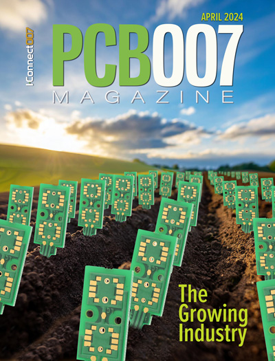
The Growing Industry
In this issue of PCB007 Magazine, we talk with leading economic experts, advocacy specialists in Washington, D.C., and PCB company leadership to get a well-rounded picture of what’s happening in the industry today. Don’t miss it.

The Sustainability Issue
Sustainability is one of the most widely used terms in business today, especially for electronics and manufacturing but what does it mean to you? We explore the environmental, business, and economic impacts.

The Fabricator’s Guide to IPC APEX EXPO
This issue previews many of the important events taking place at this year's show and highlights some changes and opportunities. So, buckle up. We are counting down to IPC APEX EXPO 2024.
- Articles
- Columns
Search Console
- Links
- Events
||| MENU - pcb007 Magazine
A Fractal Conversation with Jim Howard and Greg Lucas
January 15, 2019 | Barry Matties and Andy Shaughnessy, I-Connect007Estimated reading time: 3 minutes
Veteran PCB technologists Jim Howard and Greg Lucas have made an interesting discovery: Certain shapes of copper planes make a PCB run more efficiently than other shapes, a process they dubbed fractal design. It doesn’t appear to cost a penny more, and testing suggests that fractal design techniques could eliminate edge noise.
Barry Matties and Andy Shaughnessy asked Jim and Greg to discuss the fractal design process, as well as some of the advantages of using this technique on your next PCB design.
Barry Matties: Gentlemen, tell us how you all got started with fractals and fractal design.
Jim Howard: Greg and I were in the midst of developing a technology known as buried capacitance, and we had a number of tests that we needed to run on PCBs to determine exactly what the effects of having this very thin distributed capacitance within the board would accomplish. We discovered some effects that really didn't gel with what we were doing at that time, but they were of interest.
A few years later, we went back and thought, "These things could be useful," because we discovered that certain shapes on the copper planes of the PCBs—which, at that time, were only dictated by anti-pads and various cuts and things in the copper—either increased or decreased its ability to operate efficiently as a power/ground plane. We didn't know precisely what that effect was.
Then, I spent a few years working for a Chinese company developing some technology for them, and they wanted to see if this was something that I could work on in the future. I found we could create an effect with a specific shape of putting anti-pads, cuts, and other things where we wanted to, but the problem was that no designer was ever going to let you do that. That's an impossible scenario.
So, I discarded that for a moment, and after I left that company as their technical director, I started to think about this particular problem again. I thought, "What related fields can I get information from?" because as an engineer, I can never be too proud to beg. I started investigating unusual bits of science, came across fractals, and immediately recognized the fractals exemplified the patterns we had been creating in their simplest form. The thing I was looking at, at the time, was a Cantor set, which is one of the very early fractal forms.
I researched that, talked to Greg about it, and he thought about it for a while. Then, we realized, "Hey, there's a reason to pursue this." We initially pursued it from the point of view of something very simple that we could initially find a reason for: If we could etch this around the outside of a PCB, perhaps we could reduce the noise given off by the edges of the board. Edge noise was a significant issue with buried capacitance. We started working with it and developing some IP to give us a history in the field, and also to serve as a vehicle for further study.
Next, we created some samples. We went through testing in Silicon Valley at Dr. Earl McCune's laboratory. We did a lot of analysis with Dr. McCune. From that, we derived and sent the samples that gave us the very most interesting results to an FCC testing laboratory with a set of engineers at that end to help us interpret the responses. The responses were as we expected in terms of reducing the noise from the PCB for virtually no cost or no cost that we could think of.
To read this entire interview, which appeared in the December 2018 issue of Design007 Magazine, click here.
Suggested Items
Insulectro’s 'Storekeepers' Extend Their Welcome to Technology Village at IPC APEX EXPO
04/03/2024 | InsulectroInsulectro, the largest distributor of materials for use in the manufacture of PCBs and printed electronics, welcomes attendees to its TECHNOLOGY VILLAGE during this year’s IPC APEX EXPO at the Anaheim Convention Center, April 9-11, 2024.
ENNOVI Introduces a New Flexible Circuit Production Process for Low Voltage Connectivity in EV Battery Cell Contacting Systems
04/03/2024 | PRNewswireENNOVI, a mobility electrification solutions partner, introduces a more advanced and sustainable way of producing flexible circuits for low voltage signals in electric vehicle (EV) battery cell contacting systems.
Heavy Copper PCBs: Bridging the Gap Between Design and Fabrication, Part 1
04/01/2024 | Yash Sutariya, Saturn Electronics ServicesThey call me Sparky. This is due to my talent for getting shocked by a variety of voltages and because I cannot seem to keep my hands out of power control cabinets. While I do not have the time to throw the knife switch to the off position, that doesn’t stop me from sticking screwdrivers into the fuse boxes. In all honesty, I’m lucky to be alive. Fortunately, I also have a talent for building high-voltage heavy copper circuit boards. Since this is where I spend most of my time, I can guide you through some potential design for manufacturability (DFM) hazards you may encounter with heavy copper design.
Trouble in Your Tank: Supporting IC Substrates and Advanced Packaging, Part 5
03/19/2024 | Michael Carano -- Column: Trouble in Your TankDirect metallization systems based on conductive graphite or carbon dispersion are quickly gaining acceptance worldwide. Indeed, the environmental and productivity gains one can achieve with these processes are outstanding. In today’s highly competitive and litigious environment, direct metallization reduces costs associated with compliance, waste treatment, and legal issues related to chemical exposure. What makes these processes leaders in the direct metallization space?
AT&S Shines with Purest Copper on World Recycling Day
03/18/2024 | AT&SThe Styrian microelectronics specialist AT&S is taking World Recycling Day as an opportunity to review the progress that has been made in recent months at its sites around the world in terms of the efficient use of resources:


