


 It’s Only Common Sense: OCCAM—the Time Is Now
 Marcy's Musings: The Growing Industry
 Dan’s Biz Bookshelf: Seeing the How
Decreasing Bend Radius and Improving Reliability—Part I
October 11, 2019 | Kelsey Smith, All FlexEstimated reading time: 1 minute
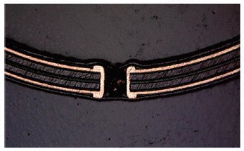
Application: Design guidelines to improve the flexibility and reliability of flexible circuits.
Many of the issues that arise when using a flex circuit come from a lack of knowledge about how to properly design one, especially when the circuit is required to bend. Many novices will design a circuit that calls for bending the flex in too tight of a bend radius, which can cause damage to the circuit and lower the reliability of the end product. This series of articles will focus on the seven key aspects to consider when designing for maximum durability and maximum “flexibility.” It is important to know that because flexibility is a relative term, this study will instead use the phrase "reducing bend radius." Here are two of the seven design strategies (please see Part II and Part III for more tips):
1. Reduce overall thickness:
IPC guidelines typically list minimum bend radius of 6X the circuit thickness for single-sided flex, 10X for double-sided flex, and 20X for multiple layer flex. The area of focus is the thickness where flexing or bending will occur, which should be only in a location with conductors and not plated through-holes. Thickness can best be reduced by:
A. Using thinner copper
B. Using adhesive-less base materials
C. Stagger conductors
D. Specifying button plating or pads only plating
Any flex circuit with plated through-holes will need to be either panel plated or button plated. Button plating is preferred because it only plates the vias and leaves the conductors un-plated and which does not increase the thickness.
2. Use only rolled annealed (RA) copper:
There are two common types of copper; rolled annealed (RA) and electro-deposited (ED) copper.
A. Rolled annealed copper is best for achieving a tighter bend radius.
B. It is also important for you to put on your drawings the direction of the grain in relation to where the tight bending will occur.
Go to Part two of this article.
Share on:


Suggested Items
Insulectro’s 'Storekeepers' Extend Their Welcome to Technology Village at IPC APEX EXPO
04/03/2024 | InsulectroInsulectro, the largest distributor of materials for use in the manufacture of PCBs and printed electronics, welcomes attendees to its TECHNOLOGY VILLAGE during this year’s IPC APEX EXPO at the Anaheim Convention Center, April 9-11, 2024.
ENNOVI Introduces a New Flexible Circuit Production Process for Low Voltage Connectivity in EV Battery Cell Contacting Systems
04/03/2024 | PRNewswireENNOVI, a mobility electrification solutions partner, introduces a more advanced and sustainable way of producing flexible circuits for low voltage signals in electric vehicle (EV) battery cell contacting systems.
Heavy Copper PCBs: Bridging the Gap Between Design and Fabrication, Part 1
04/01/2024 | Yash Sutariya, Saturn Electronics ServicesThey call me Sparky. This is due to my talent for getting shocked by a variety of voltages and because I cannot seem to keep my hands out of power control cabinets. While I do not have the time to throw the knife switch to the off position, that doesn’t stop me from sticking screwdrivers into the fuse boxes. In all honesty, I’m lucky to be alive. Fortunately, I also have a talent for building high-voltage heavy copper circuit boards. Since this is where I spend most of my time, I can guide you through some potential design for manufacturability (DFM) hazards you may encounter with heavy copper design.
Trouble in Your Tank: Supporting IC Substrates and Advanced Packaging, Part 5
03/19/2024 | Michael Carano -- Column: Trouble in Your TankDirect metallization systems based on conductive graphite or carbon dispersion are quickly gaining acceptance worldwide. Indeed, the environmental and productivity gains one can achieve with these processes are outstanding. In today’s highly competitive and litigious environment, direct metallization reduces costs associated with compliance, waste treatment, and legal issues related to chemical exposure. What makes these processes leaders in the direct metallization space?
AT&S Shines with Purest Copper on World Recycling Day
03/18/2024 | AT&SThe Styrian microelectronics specialist AT&S is taking World Recycling Day as an opportunity to review the progress that has been made in recent months at its sites around the world in terms of the efficient use of resources: