-

- News
- Books
Featured Books
- smt007 Magazine
Latest Issues
Current Issue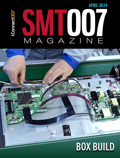
Box Build
One trend is to add box build and final assembly to your product offering. In this issue, we explore the opportunities and risks of adding system assembly to your service portfolio.
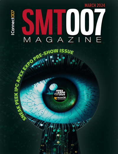
IPC APEX EXPO 2024 Pre-show
This month’s issue devotes its pages to a comprehensive preview of the IPC APEX EXPO 2024 event. Whether your role is technical or business, if you're new-to-the-industry or seasoned veteran, you'll find value throughout this program.

Boost Your Sales
Every part of your business can be evaluated as a process, including your sales funnel. Optimizing your selling process requires a coordinated effort between marketing and sales. In this issue, industry experts in marketing and sales offer their best advice on how to boost your sales efforts.
- Articles
- Columns
Search Console
- Links
- Events
||| MENU - smt007 Magazine
Miniaturization Continues: Day 3 productronica Coverage
November 15, 2019 | I-Connect007 Editorial TeamEstimated reading time: 1 minute
The conversations on day 3 of productronica continued, including topics such as flexibility, 5G capabilities, and increased data and intelligence. The theme from test and inspection equipment providers included increased capabilities in sensing, material handling, and visual inspection technologies. And through it all, one common perspective emerged time and time again: PCB manufacturing is now approaching the levels of line, trace, and component density that were once limited to the surface of a silicon wafer.
What was once a level of precision relegated to the smooth, mirror-like surface of a wafer slice and then sealed in a package, now is expected upon the relatively rough, uneven, and flexible surface of today’s newest materials. Organizations—equipment manufacturers, university research consortia, industry standards organizations, and more—are all collaborating to bring these capabilities to PCB fabrication.
On Thursday, I-Connect007 caught up with the likes of Isola, Koh Young, CyberOptics, ESI, PVA, Mirtec, Hitachi High-Tech, Indubond, Vayo Technology, Meyer Burger, Agfa, Polar, Rogers, and Orbotech. We also report on the IPC Hand Soldering World Championships, which concluded—with much excitement—Thursday afternoon. We will have coverage of the event and the awards ceremony soon.
One more day of productronica coverage still to come.
Suggested Items
Real Time with... IPC APEX EXPO 2024: Exploring IPC's PCB Design Courses with Kris Moyer
04/18/2024 | Real Time with...IPC APEX EXPOGuest Editor Kelly Dack and IPC instructor Kris Moyer discuss IPC's PCB design training and education offerings. They delve into course topics such as design fundamentals, mil/aero, rigid-flex, RF design, and advanced design concepts. They also highlight material selection for high-speed design, thermal management, and dissipation techniques. The interview wraps up with details about how to access these courses online.
IPC Bestows Posthumous Hall of Fame Award to Industry Icon Michael Ford
04/18/2024 | IPCIPC honored the late Michael Ford, Aegis Software, for his extraordinary contributions to the global electronics manufacturing industry with the IPC Raymond E. Pritchard Hall of Fame Award at IPC APEX EXPO 2024. IPC’s most prestigious honor, the Hall of Fame Award is given to individuals who have provided exceptional service and advancement to IPC and the electronics industry. Ford, an industry leader and valued IPC volunteer, died suddenly in January 2024.
Two Industry Rising Stars Recognized at IPC APEX EXPO 2024
04/17/2024 | IPCTwo of the industry’s best and brightest were presented with an IPC Rising Star Award at IPC APEX EXPO 2024 in recognition of their leadership roles and support of IPC standards, education, advocacy, and solutions to industry challenges. Award recipients were Naim Kapadia and Michael Schleicher.
Two Long-time IPC Volunteers Receive Dieter Bergman IPC Fellowship Award
04/17/2024 | IPCThe Dieter Bergman IPC Fellowship award was presented to two IPC volunteers at IPC APEX EXPO 2024. The award recipients have fostered a collaborative spirit, made significant contributions to standards development, and have consistently demonstrated a commitment to global standardization efforts. Tiberiu Baranyi and Zhiman Chen were chosen as award recipients as they embody the work ethic and spirit of the late Dieter Bergman, an industry pioneer and icon. As part of the award, they bestowed Dieter Bergman Memorial Scholarships to the university or college of their choice.
Real Time with... IPC APEX EXPO 2024: MYCRONIC's Evolution and New Solutions
04/17/2024 | Real Time with...IPC APEX EXPOHenry Crandall interviews Kevin Clue, the vice president of global sales for MYCRONIC's High Flex division. They discuss the company's evolution, emphasizing its strong customer relationships and its role as a versatile, turnkey solution provider. Kevin unveils new solutions launched at IPC APEX EXPO, including an AI-integrated inspection system and the A40 pick-and-place platform. The conversation also touches on the increased use of AI and deep learning.
