


 The Right Approach: I Hear the Train A Comin'
 It’s Only Common Sense: OCCAM—the Time Is Now
 Marcy's Musings: The Growing Industry
HD-BNC Port PCB Connectors Increase Connectivity Density
May 18, 2020 | Amphenol RFEstimated reading time: Less than a minute
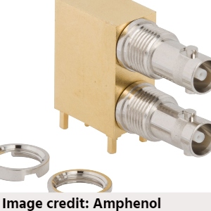
Amphenol RF is pleased to introduce HD-BNC dual port PCB jacks into an already broad portfolio of 12G optimized interconnects. This new connector configuration allows for dual-port termination and increases connector density while saving valuable PCB real estate, eliminating the need for risers or mezzanine connectors. The dual port interface is ideal for 4K or ultra-HD broadcast applications and meets the latest SMPTE specifications for 12G broadcast.
The HD-BNC dual port PCB jacks feature the popular bayonet style coupling mechanism and offer stable electrical performance though 18 GHz. The connector contacts are gold plated beryllium copper, and bodies are matte tin plated zinc die-cast, or gold plated machined brass. Both designs have a secure bulkhead mounting feature. These jacks are available as both stacked and staggered mount configurations for additional versatility.
In addition to 12G HD-BNC products, Amphenol RF also offers multiple 12G capable configurations of the popular BNC connector and most recently, MCX connectors. Adapters and fixed length cable assemblies are also available.
Share on:


Suggested Items
TTM Celebrates the Grand Opening of Its First Manufacturing Facility in Penang
04/25/2024 | TTM Technologies, Inc.TTM Technologies, Inc., a leading global manufacturer of technology solutions including mission systems, radio frequency (RF) components and RF microwave/microelectronic assemblies, and quick-turn and technologically advanced printed circuit boards (PCBs), officially opened its first manufacturing plant in Penang, Malaysia with an investment of USD200 million (approximately RM958 million).
Designer’s Notebook: What Designers Need to Know About Manufacturing, Part 2
04/24/2024 | Vern Solberg -- Column: Designer's NotebookThe printed circuit board (PCB) is the primary base element for providing the interconnect platform for mounting and electrically joining electronic components. When assessing PCB design complexity, first consider the component area and board area ratio. If the surface area for the component interface is restricted, it may justify adopting multilayer or multilayer sequential buildup (SBU) PCB fabrication to enable a more efficient sub-surface circuit interconnect.
Elevating PCB Design Engineering With IPC Programs
04/24/2024 | Cory Blaylock, IPCIn a monumental stride for the electronics manufacturing industry, IPC has successfully championed the recognition of the PCB Design Engineer as an official occupation by the U.S. Department of Labor (DOL). This pivotal achievement not only underscores the critical role of PCB design engineers within the technology landscape, but also marks the beginning of a transformative journey toward nurturing a robust, skilled workforce ready to propel our industry into the future.
IPC Design Competition Champion Crowned at IPC APEX EXPO 2024
04/24/2024 | IPCAt IPC APEX EXPO 2024 in Anaheim, California, five competitors squared off to determine who was the best of the best at PCB design.
Real Time with... IPC APEX EXPO 2024: all4-PCB, A Premier Solution Provider for the PCB Industry
04/22/2024 | Real Time with...IPC APEX EXPOIn the PCB industry, all4-PCB, is a top-tier equipment supplier and process solution provider. Ralph Jacobo highlights the active market and the demand for high-quality equipment, discusses their existing customers, investment in advanced substrates, and smaller board shops.