


 It’s Only Common Sense: OCCAM—the Time Is Now
 Marcy's Musings: The Growing Industry
 Dan’s Biz Bookshelf: Seeing the How
Samsung Electronics Expands its Foundry Capacity with A New Production Line in Pyeongtaek, Korea
May 21, 2020 | Business WireEstimated reading time: 1 minute
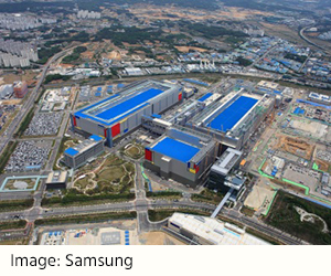
Samsung Electronics Co., Ltd., a world leader in advanced semiconductor technology, today announced plans to boost its foundry capacity at the company's new production line in Pyeongtaek, Korea, to meet growing global demand for cutting-edge extreme ultraviolet (EUV) solutions.
The new foundry line, which will focus on EUV-based 5 nanometer (nm) and below process technology, has just commenced construction this month and is expected to be in full operation in the second half of 2021. It will play a pivotal role as Samsung aims to expand the use of state-of-the-art process technologies across a myriad of current and next generation applications, including 5G, high-performance computing (HPC) and artificial intelligence (AI).
“This new production facility will expand Samsung’s manufacturing capabilities for sub-5nm process and enable us to rapidly respond to the increasing demand for EUV-based solutions,” said Dr. ES Jung, President and Head of Foundry Business at Samsung Electronics. “We remain committed to addressing the needs of our customers through active investments and recruitment of talents. This will enable us to continue to break new ground while driving robust growth for Samsung’s foundry business.”
Following the initial mass production of the EUV-based 7nm process in early 2019, Samsung recently added a new EUV-dedicated V1 line in Hwaseong, Korea, to its global foundry network. With the new Pyeongtaek facility starting full operation in 2021, Samsung’s foundry capacity based on EUV is expected to increase significantly.
Samsung is scheduled to start mass production of 5nm EUV process in the Hwaseong fab in the second half of this year.
With the addition of the Pyeongtaek fab, Samsung will have a total of seven foundry production lines located in South Korea and the United States, comprised of six 12-inch lines and one 8-inch line.
Share on:


Suggested Items
KYZEN to Promote Pair of Stencil Cleaning Chemistries at SMTA Ciudad Jaurez Expo & Tech Forum
04/25/2024 | KYZEN'KYZEN, the global leader in innovative environmentally friendly cleaning chemistries, will exhibit at the SMTA Ciudad Juarez Expo & Tech Forum, scheduled to take place Thursday, May 9, 2024 at the Injectronic Convention Center in Ciudad Jaurez, Chihuahua, Mexico. During the event the KYZEN Clean Team will focus on understencil cleaning products KYZEN E5631J and CYBERSOLV C8882.
Cadence, TSMC Collaborate on Wide-Ranging Innovations to Transform System and Semiconductor Design
04/25/2024 | Cadence Design SystemsCadence Design Systems, Inc. and TSMC have extended their longstanding collaboration by announcing a broad range of innovative technology advancements to accelerate design, including developments ranging from 3D-IC and advanced process nodes to design IP and photonics.
Listen Up! The Intricacies of PCB Drilling Detailed in New Podcast Episode
04/25/2024 | I-Connect007In episode 5 of the podcast series, On the Line With: Designing for Reality, Nolan Johnson and Matt Stevenson continue down the manufacturing process, this time focusing on the post-lamination drilling process for PCBs. Matt and Nolan delve into the intricacies of the PCB drilling process, highlighting the importance of hole quality, drill parameters, and design optimization to ensure smooth manufacturing. The conversation covers topics such as drill bit sizes, aspect ratios, vias, challenges in drilling, and ways to enhance efficiency in the drilling department.
Designer’s Notebook: What Designers Need to Know About Manufacturing, Part 2
04/24/2024 | Vern Solberg -- Column: Designer's NotebookThe printed circuit board (PCB) is the primary base element for providing the interconnect platform for mounting and electrically joining electronic components. When assessing PCB design complexity, first consider the component area and board area ratio. If the surface area for the component interface is restricted, it may justify adopting multilayer or multilayer sequential buildup (SBU) PCB fabrication to enable a more efficient sub-surface circuit interconnect.
Real Time with... IPC APEX EXPO 2024: Advancements in Laser Depaneling with LPKF
04/24/2024 | Real Time with...IPC APEX EXPOJake Benz, LPKF sales manager for North America, discusses the company's advancements in laser depaneling. LPKF has introduced a green wavelength laser for processing rigid FR-4 circuit boards, bringing significant gains in processing speeds to market. The company transitioned from IR CO2 to UV wavelength due to heat and burning issues.