


 It’s Only Common Sense: OCCAM—the Time Is Now
 Marcy's Musings: The Growing Industry
 Dan’s Biz Bookshelf: Seeing the How
Isola Opens Expanded R&D and Analytical Laboratory in Arizona
June 19, 2020 | PR NewswireEstimated reading time: 2 minutes
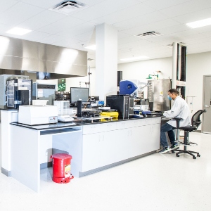
Isola, designer and developer of copper-clad laminates and fabrication materials for multi-layer printed circuit boards (PCBs), has officially opened an expansive R&D and analytical services laboratory at the company's new global headquarters in Chandler, Ariz.
Nearly doubling the size and capacity of the testing facility enables enhanced product development, material qualification, application engineering, and technical support to printed circuit board fabricators and the OEMs they serve. Access to Isola's testing facilities throughout the world is a complimentary service offered to Isola customers. The Arizona operations also include a 118,000-square-foot quick-turnaround manufacturing facility to accommodate the industry's agile demands.
In the R&D and analytical lab, Isola incorporated a refined and optimized workflow with dedicated space for each testing process. These dedicated spaces provide a more optimal working environment for Isola technicians, chemists, and researchers, benefiting customers through enhanced efficiency. The lab's highly trained team conducts electrical, thermal, and mechanical characterizations of resin components and PCB laminate materials used in the production of printed circuit boards and uses advanced test equipment to achieve accurate results in a rapid response environment. Known as the Johann Schumacher Laboratories, the facility is named for an Isola technical fellow and engineer, who—throughout his 35 years with the company—has developed numerous innovations.
"The North American PCB market is all about quick turnaround and high complexity. Isola's investment in local testing and analysis complements the investments our customers have made to meet the growing complexity of the products designed by OEMs," said Travis Kelly, President & CEO. "The expanded R&D and analytical services laboratory furthers our ability to both improve analytical capability and maintain quick turnaround times."
The lab includes a variety of testing equipment—from Fourier Transform Infrared Spectroscopy (FTIR) and Scanning Electron Microscopy (SEM) analysis for identification of contaminants to microsection equipment used for evaluation of printed circuit board integrity after thermal excursions. The thermal analysis area consists of 17 instruments that measure thermal properties as a function of temperature while specimens are subject to a controlled temperature program.
"While thermal analysis is one of the lab's most in-demand services, the global Johann Schumacher Laboratories network, with locations in the U.S., Singapore, and Germany, helps customers work through various challenges related to their products," said Jenny Inocencio, Sr. Manager Global JSL. "Our cross-trained professionals—many of whom also have experience in the manufacturing environment—understand the full process of how materials are assembled, bring keen insights to identifying problems, and confidently consider different approaches. Customers have the advantage of leveraging our global network as their business needs change and during unexpected market events."
Isola's global R&D and analytical laboratory team is led by Ed Kelley, Chief Technology Officer, Phil Whalen, Chief New Product Development and Strategy Officer, Drew Rocha, R&D Manager; and Jenny Inocencio, Senior Manager, Global JSL
Share on:


Suggested Items
Insulectro’s 'Storekeepers' Extend Their Welcome to Technology Village at IPC APEX EXPO
04/03/2024 | InsulectroInsulectro, the largest distributor of materials for use in the manufacture of PCBs and printed electronics, welcomes attendees to its TECHNOLOGY VILLAGE during this year’s IPC APEX EXPO at the Anaheim Convention Center, April 9-11, 2024.
ENNOVI Introduces a New Flexible Circuit Production Process for Low Voltage Connectivity in EV Battery Cell Contacting Systems
04/03/2024 | PRNewswireENNOVI, a mobility electrification solutions partner, introduces a more advanced and sustainable way of producing flexible circuits for low voltage signals in electric vehicle (EV) battery cell contacting systems.
Heavy Copper PCBs: Bridging the Gap Between Design and Fabrication, Part 1
04/01/2024 | Yash Sutariya, Saturn Electronics ServicesThey call me Sparky. This is due to my talent for getting shocked by a variety of voltages and because I cannot seem to keep my hands out of power control cabinets. While I do not have the time to throw the knife switch to the off position, that doesn’t stop me from sticking screwdrivers into the fuse boxes. In all honesty, I’m lucky to be alive. Fortunately, I also have a talent for building high-voltage heavy copper circuit boards. Since this is where I spend most of my time, I can guide you through some potential design for manufacturability (DFM) hazards you may encounter with heavy copper design.
Trouble in Your Tank: Supporting IC Substrates and Advanced Packaging, Part 5
03/19/2024 | Michael Carano -- Column: Trouble in Your TankDirect metallization systems based on conductive graphite or carbon dispersion are quickly gaining acceptance worldwide. Indeed, the environmental and productivity gains one can achieve with these processes are outstanding. In today’s highly competitive and litigious environment, direct metallization reduces costs associated with compliance, waste treatment, and legal issues related to chemical exposure. What makes these processes leaders in the direct metallization space?
AT&S Shines with Purest Copper on World Recycling Day
03/18/2024 | AT&SThe Styrian microelectronics specialist AT&S is taking World Recycling Day as an opportunity to review the progress that has been made in recent months at its sites around the world in terms of the efficient use of resources: