-

- News
- Books
Featured Books
- pcb007 Magazine
Latest Issues
Current Issue
The Growing Industry
In this issue of PCB007 Magazine, we talk with leading economic experts, advocacy specialists in Washington, D.C., and PCB company leadership to get a well-rounded picture of what’s happening in the industry today. Don’t miss it.
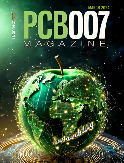
The Sustainability Issue
Sustainability is one of the most widely used terms in business today, especially for electronics and manufacturing but what does it mean to you? We explore the environmental, business, and economic impacts.

The Fabricator’s Guide to IPC APEX EXPO
This issue previews many of the important events taking place at this year's show and highlights some changes and opportunities. So, buckle up. We are counting down to IPC APEX EXPO 2024.
- Articles
- Columns
Search Console
- Links
- Events
||| MENU - pcb007 Magazine
Developments in Low-Loss Substrates for High-Frequency Applications
March 29, 2022 | Alun Morgan, Ventec International GroupEstimated reading time: 2 minutes
The electronics industry as we know it today can trace its birth to the creation of the first integrated circuit in 1958, although conception occurred 10 years earlier with the invention of the transistor. That first IC contained a single transistor and four passive components. To say things have come a long way since then is a huge understatement.
Only one thing may have matched the meteoric pace of progress in our industry—market expectation. Exponential advancement has become the norm, and this is now achieved through an aggregation of improvements, rather than a large leap in one aspect such as chip lithography (Moore’s Law), or processor frequency scaling (Dennard).
It’s a small step from acknowledging this reality to adopting a holistic view that acknowledges the contribution each aspect of the system can make toward the overall performance and that seeks to optimize the interactions between them. Accordingly, in cutting-edge applications, we no longer have the luxury of treating the PCB as merely a medium for mounting and connecting components. At high signal speeds in particular, the properties of the substrate, copper foil, and trace geometries govern whether the system can deliver the required performance.
Many within the industry already understand that the PCB has become a high-tech component in itself, particularly those departments working on applications in automotive radar, 5G, and satellite communications at multi-gigahertz frequencies.
Low-Loss Substrates
These applications are operating close to the limits of the capabilities typical materials can offer. Resistive loss mechanisms, including the skin effect in copper conductors and dielectric losses due to the molecular dipole moment in the insulating substrate need to be understood and carefully managed. The cumulative effect of the tiny losses in signal energy and associated thermal dissipation incurred with every signaling transition becomes appreciable. If not properly addressed, these losses demand more powerful transmitters, more sensitive receivers, and extra thermal management than are practicable within the typical constraints on power, as well as size, weight, and cost that usually prevail.
There are growing demands for low-loss substrates to address high-performance systems, spanning applications from high-end servers and telecom infrastructure all the way to mmWave 5G, satellite, and radar applications.
By enhancing aspects of PCB laminates, it has been possible to produce low-loss substrates that can handle demanding applications in data centers and telecom switches, for example. Optimizing the fiber weave effectively minimizes micro-variabilities in signal-path characteristics that cause distortions such as signal skew, which ultimately give rise to excessive noise and signaling errors. Attributes such as drilling performance and resistance to CAF (conductive anodic filament) formation are also improved.
For applications operating at the highest frequencies in use today, ceramic-filled and PTFE-based materials are achieving the lowest loss factors in the industry. The molecular structure of PTFE (polytetrafluoroethylene) arranges fluorine atoms as spirals around the carbon backbone to create a rod-like stiff cylindrical shape that has no dipole moment. This absence of any dipole moment negates the oscillations set up in conventional substrate dielectrics due to repeated polarization caused by signal current. This is manifested as an extremely low dissipation factor (Df) that helps to reduce signal losses.
To read this entire article, which appeared in the March 2022 issue of PCB007 Magazine, click here.
Suggested Items
Designer’s Notebook: What Designers Need to Know About Manufacturing, Part 2
04/24/2024 | Vern Solberg -- Column: Designer's NotebookThe printed circuit board (PCB) is the primary base element for providing the interconnect platform for mounting and electrically joining electronic components. When assessing PCB design complexity, first consider the component area and board area ratio. If the surface area for the component interface is restricted, it may justify adopting multilayer or multilayer sequential buildup (SBU) PCB fabrication to enable a more efficient sub-surface circuit interconnect.
Insulectro’s 'Storekeepers' Extend Their Welcome to Technology Village at IPC APEX EXPO
04/03/2024 | InsulectroInsulectro, the largest distributor of materials for use in the manufacture of PCBs and printed electronics, welcomes attendees to its TECHNOLOGY VILLAGE during this year’s IPC APEX EXPO at the Anaheim Convention Center, April 9-11, 2024.
ENNOVI Introduces a New Flexible Circuit Production Process for Low Voltage Connectivity in EV Battery Cell Contacting Systems
04/03/2024 | PRNewswireENNOVI, a mobility electrification solutions partner, introduces a more advanced and sustainable way of producing flexible circuits for low voltage signals in electric vehicle (EV) battery cell contacting systems.
Heavy Copper PCBs: Bridging the Gap Between Design and Fabrication, Part 1
04/01/2024 | Yash Sutariya, Saturn Electronics ServicesThey call me Sparky. This is due to my talent for getting shocked by a variety of voltages and because I cannot seem to keep my hands out of power control cabinets. While I do not have the time to throw the knife switch to the off position, that doesn’t stop me from sticking screwdrivers into the fuse boxes. In all honesty, I’m lucky to be alive. Fortunately, I also have a talent for building high-voltage heavy copper circuit boards. Since this is where I spend most of my time, I can guide you through some potential design for manufacturability (DFM) hazards you may encounter with heavy copper design.
Trouble in Your Tank: Supporting IC Substrates and Advanced Packaging, Part 5
03/19/2024 | Michael Carano -- Column: Trouble in Your TankDirect metallization systems based on conductive graphite or carbon dispersion are quickly gaining acceptance worldwide. Indeed, the environmental and productivity gains one can achieve with these processes are outstanding. In today’s highly competitive and litigious environment, direct metallization reduces costs associated with compliance, waste treatment, and legal issues related to chemical exposure. What makes these processes leaders in the direct metallization space?
