


 It’s Only Common Sense: OCCAM—the Time Is Now
 Marcy's Musings: The Growing Industry
 Dan’s Biz Bookshelf: Seeing the How
Bowman's Micro XRF Measures Smallest Features in Wafers, Microelectronics
June 6, 2022 | BowmanEstimated reading time: 1 minute
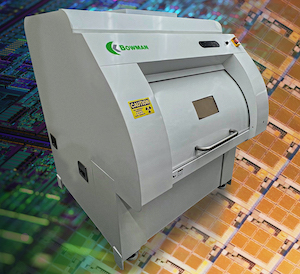
Bowman has introduced an important addition to its suite of precision XRF instruments used in the PCB, semiconductor and microelectronics industries.
The Bowman A Series Micro XRF quickly measures the smallest features on semiconductors and microelectronics. It accommodates very large PCB panels, and wafers of any size, for full sample coverage and multi-point programmable automation.
Poly-capillary optics focus the X-ray beam to 7.5 µm FWHM, the world’s smallest for XRF coating thickness analysis. A 140X magnification camera measures features on that scale; a secondary, low magnification camera provides live-viewing of samples and “birds-eye” macro-view imaging. Bowman’s proprietary dual-camera system lets operators see the entire part, click the image to zoom with the high-mag camera, and quickly identify the feature of interest.
A programmable X-Y stage with movement of 23.6 in (600 mm) in each direction can handle the largest samples in the industry. The stage has precision down to +/- 1 µm for each axis, and is used to select and measure multiple points; Bowman pattern recognition software and auto-focus features also do this automatically. The system’s 3D mapping capability can be used to view the topography of ENIG, ENEPIG, EPIG and other elite processes.
A Series instruments include 7.5 µm optics with molybdenum anode tube (chromium and tungsten also available) and a high-resolution, large-window Silicon Drift Detector (SDD) which processes more than 2 million counts per second. SDDs are the standard, industry-wide, for complex thin films. The high count rate capability is key to achieving a low minimum detection limit (MDL) and highest spectral resolution.
A Series systems are distinctive in that they are cleanroom-ready, have the largest semiconductor stage movement on the market, and are supported worldwide by a service network that provides same-day response for every benchtop XRF requirement. Equipment evaluation, selection, commissioning, maintenance and modernization is available for users of Bowman instruments, as well as other major XRF brands.
Share on:


Suggested Items
Inkjet Solder Mask ‘Has Arrived’
04/10/2024 | Pete Starkey, I-Connect007I was delighted to be invited to attend an interactive webinar entitled “Solder Mask Coating Made Easy with Additive Manufacturing,” hosted by SUSS MicroTec Netherlands in Eindhoven. The webinar was introduced and moderated by André Bodegom, managing director at Adeon Technologies, and the speakers were Mariana Van Dam, senior product manager PCB imaging solutions at AGFA in Belgium; Ashley Steers, sales manager at Electra Polymers in the UK; and Dr. Luca Gautero, product manager at SUSS MicroTec Netherlands.
NetVia Group Acquires Direct Imaging from Mivatek
04/09/2024 | Miva TechnologiesMiva Technologies is pleased to announce NetVia Group, Irving, TX has acquired a new Miva 2400NG Dual Tray Direct Imaging System with 30-micron capabilities for inner, outer and soldermask imaging.
Teledyne to Acquire Adimec
02/13/2024 | TeledyneTeledyne Technologies Incorporated announced that it has entered into an agreement to acquire Adimec Holding B.V. and its subsidiaries.
Real Time with... productronica 2023: MivaTek Global Advances Technology With High-res Imaging System
12/08/2023 | Real Time with...productronicaMivaTek's Brendan Hogan talks about how the company employs Digitally Adaptive Rasterization Technology (DART) in their high-res imaging equipment. He also shares how the blurred line between semiconductors and microelectronics is driving broader application of the imaging process.
Keysight Enables Validation of Arbe 4D Imaging Radar Chipset
11/30/2023 | Keysight Technologies, Inc.Keysight Technologies, Inc. announces that Arbe has selected the E8719A Radar Target Solution (RTS) to test the Arbe 4D imaging radar chipset for automotive applications.