


 Marcy's Musings: The Growing Industry
 It’s Only Common Sense: Here’s What To Do After IPC APEX EXPO 2024
 Dan’s Biz Bookshelf: Seeing the How
InnovationLab Demonstrates Breakthrough PCB Production Method Based on Additive Manufacturing
August 8, 2022 | InnovationLabEstimated reading time: 1 minute
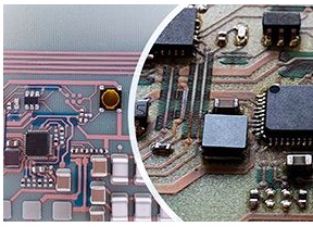
InnovationLab, the expert in printed electronics "from lab to fab", announces it has achieved a breakthrough in additive manufacturing of printed circuit boards (PCBs), helping meet higher environmental standards for electronics production while also reducing costs.
Within the research project SmartEEs2, funded by Horizon 2020, InnovationLab and its partner ISRA have developed a novel manufacturing process for copper-based solderable circuits. The circuits are screen printed and are compatible with conventional reflow processes.
Producing printed electronics is an additive process that does not use toxic etchants, and runs at comparatively low temperatures of around 150ºC, thus reducing energy consumption. Moreover, the substrates used in additive PCB manufacturing are up to 15 times thinner, compared to conventional techniques, which reduces material consumption and means the production process has less waste.
InnovationLab has so far produced a physical prototype, which includes all the important blocks of a smart label. It uses a copper ink to ensure high conductivity. Component mounting can be done in a conventional reflow soldering process, which enables manufacturers to switch to the new technology without investment in new equipment.
Multilayer layer printing, metal and dielectric, was used to produce the target functionality: a low power temperature sensor and logger, an NFC communication interface via a printed antenna, and a compact battery that is charged from a printed solar cell, making the device completely self-sufficient. The new process can produce both standard and flexible PCBs with up to four layers and can be used in product and process development for hybrid electronics.
Dr. Janusz Schinke, Head of Printed Electronics at InnovationLab, said, "This is a state-of-the-art production process, which will decrease costs and reduce logistical dependencies on suppliers, while delivering three key benefits for the environment: consuming fewer materials, using less energy, and producing less waste. By the end of this year, we expect to have scaled this process to high volumes, meeting customer demands of a million solderable tracks or more.”
SmartEEs2 is a European project, which is funded by the European Union’s Horizon 2020 research and innovation program. Its objective is to provide acceleration support to innovative companies for the integration of flexible and wearable electronics technologies, and thus to help European industry’s competitiveness.
Share on:


Suggested Items
IDTechEx Examines the Opportunities for Wearables in Digital Health
04/19/2024 | IDTechExIDTechEx’s report, “Digital Health and Artificial Intelligence 2024-2034: Trends, Opportunities, and Outlook”, covers this ongoing trend in the consumer health wearables market and includes analysis of the opportunities and roadmap for biometric monitoring.
ZESTRON Welcomes Whitlock Associates as New Addition to their Existing Rep Team in Florida
04/19/2024 | ZESTRONZESTRON, the leading global provider of high-precision cleaning products, services, and training solutions in the electronics manufacturing and semiconductor industries, is thrilled to announce the addition of Whitlock Associates to its esteemed network of sales representatives.
IPC Bestows Posthumous Hall of Fame Award to Industry Icon Michael Ford
04/18/2024 | IPCIPC honored the late Michael Ford, Aegis Software, for his extraordinary contributions to the global electronics manufacturing industry with the IPC Raymond E. Pritchard Hall of Fame Award at IPC APEX EXPO 2024. IPC’s most prestigious honor, the Hall of Fame Award is given to individuals who have provided exceptional service and advancement to IPC and the electronics industry. Ford, an industry leader and valued IPC volunteer, died suddenly in January 2024.
SEMI Applauds U.S. Chips Act Award for Samsung Electronics Facilities to Strengthen Domestic Semiconductor Supply Chain
04/17/2024 | SEMISEMI, the industry association serving the global electronics design and manufacturing supply chain, applauded the United States Department of Commerce’s announcement of a Preliminary Memorandum of Terms for an award under the CHIPS and Science Act to support the expansion of Samsung Electronics’ presence in Texas and the company’s development and production of leading-edge chips.
Northrop Grumman honors Calumet Electronics with Supplier Excellence Award
04/17/2024 | Calumet ElectronicsNorthrop Grumman Corporation has recognized Calumet Electronics during the company’s 2024 Supplier Excellence Awards for “exceptional performance and unwavering commitment to delivering with excellence.” Calumet is one of 70 suppliers recognized from across the globe. In its award category of “Supplier Strategic Excellence,” Calumet was honored alongside global corporations such as Amazon Web Services, Dell Technologies, and Eaton Corporation.