


 Marcy's Musings: The Growing Industry
 It’s Only Common Sense: Here’s What To Do After IPC APEX EXPO 2024
 Dan’s Biz Bookshelf: Seeing the How
MKS Instruments Unveils Significant Investment in its Yokohama TechCenter at Expansion Ceremony
March 14, 2023 | MKS Instruments, Inc.Estimated reading time: 2 minutes
MKS Instruments, Inc., a global provider of technologies that transform our world, unveiled a significant investment in its Yokohama Technical Center (YTC) in Japan, which will enable an industry leading integrated approach to creating solutions for complex package substrate manufacturing, satisfying current requirements as well as those needed for future roadmaps.
The YTC is an integral part of the most comprehensive portfolio of global TechCenters in the industry. These TechCenters combine unique analytical capabilities, state of the art full scale equipment, and highly proficient expert teams to conduct extensive research and development, providing world-class service to more than 8,000 customers around the globe. Working closely with customers and industry partners helps anticipate the industry’s future requirements, which in turn enables MKS to help customers stay ahead in a rapidly changing environment.
The recent investment in the YTC delivers the latest capabilities for the production of next generation package substrates. Offering a unique combination, the YTC utilizes dedicated lasers, optics, and motion systems for high precision, high-speed via formation in ABF build-up laminates, in combination with the latest process chemistry and equipment for desmear and electroless copper metallization. Using the latest Equalized Curtain Flow (ECF) plating tool, the YTC is able to support customers in their yield optimization and next generation process development for advanced packaging applications.
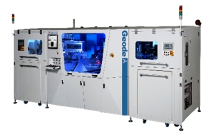
During the YTC Expansion Ceremony, Dr. John T.C. Lee, President and CEO of MKS Instruments, escorted visitors around the state-of-the-art facility showcasing the two new systems, the ESI GeodeTM A CO2 laser system and the Atotech G-Plate® plating tool, as well as demonstrating the Vitrocoat® process for Plating on Glass (PoG).
“We are highly committed to driving and leading technology development within our industries,” Dr. Lee said. “With these key installations, we are accelerating time to market through our combined capabilities, which allow us to view problems holistically and design solutions faster. This helps us to drive innovation for next generation electronic devices and offer customers and OEMs quicker development cycles for new products and materials enabling high-end SAP technology requiring <=5/5µm lines and spaces. Our unique portfolio of MKS combined services at our Yokohama technical center allows us to reduce the cycle time for a typical ABF sample from three months or more to less than one month.”
MKS Instruments’ Optimize the InterconnectSM offering drives MKS’ focus on next-generation advanced PCB and package substrate development. The investment in the YTC will further solidify MKS as a leader in the next frontier for miniaturization and complexity by enabling increasingly smaller feature sizes and offering new solutions by combining ESI laser drilling technologies with Atotech chemistry and plating equipment.
Share on:


Suggested Items
Insulectro’s 'Storekeepers' Extend Their Welcome to Technology Village at IPC APEX EXPO
04/03/2024 | InsulectroInsulectro, the largest distributor of materials for use in the manufacture of PCBs and printed electronics, welcomes attendees to its TECHNOLOGY VILLAGE during this year’s IPC APEX EXPO at the Anaheim Convention Center, April 9-11, 2024.
ENNOVI Introduces a New Flexible Circuit Production Process for Low Voltage Connectivity in EV Battery Cell Contacting Systems
04/03/2024 | PRNewswireENNOVI, a mobility electrification solutions partner, introduces a more advanced and sustainable way of producing flexible circuits for low voltage signals in electric vehicle (EV) battery cell contacting systems.
Heavy Copper PCBs: Bridging the Gap Between Design and Fabrication, Part 1
04/01/2024 | Yash Sutariya, Saturn Electronics ServicesThey call me Sparky. This is due to my talent for getting shocked by a variety of voltages and because I cannot seem to keep my hands out of power control cabinets. While I do not have the time to throw the knife switch to the off position, that doesn’t stop me from sticking screwdrivers into the fuse boxes. In all honesty, I’m lucky to be alive. Fortunately, I also have a talent for building high-voltage heavy copper circuit boards. Since this is where I spend most of my time, I can guide you through some potential design for manufacturability (DFM) hazards you may encounter with heavy copper design.
Trouble in Your Tank: Supporting IC Substrates and Advanced Packaging, Part 5
03/19/2024 | Michael Carano -- Column: Trouble in Your TankDirect metallization systems based on conductive graphite or carbon dispersion are quickly gaining acceptance worldwide. Indeed, the environmental and productivity gains one can achieve with these processes are outstanding. In today’s highly competitive and litigious environment, direct metallization reduces costs associated with compliance, waste treatment, and legal issues related to chemical exposure. What makes these processes leaders in the direct metallization space?
AT&S Shines with Purest Copper on World Recycling Day
03/18/2024 | AT&SThe Styrian microelectronics specialist AT&S is taking World Recycling Day as an opportunity to review the progress that has been made in recent months at its sites around the world in terms of the efficient use of resources: