-

- News
- Books
Featured Books
- pcb007 Magazine
Latest Issues
Current Issue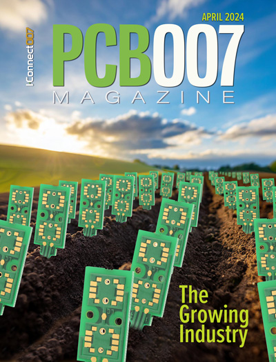
The Growing Industry
In this issue of PCB007 Magazine, we talk with leading economic experts, advocacy specialists in Washington, D.C., and PCB company leadership to get a well-rounded picture of what’s happening in the industry today. Don’t miss it.

The Sustainability Issue
Sustainability is one of the most widely used terms in business today, especially for electronics and manufacturing but what does it mean to you? We explore the environmental, business, and economic impacts.

The Fabricator’s Guide to IPC APEX EXPO
This issue previews many of the important events taking place at this year's show and highlights some changes and opportunities. So, buckle up. We are counting down to IPC APEX EXPO 2024.
- Articles
Article Highlights
- Columns
Search Console
- Links
- Events
||| MENU - pcb007 Magazine
NCAB Advocates for Advanced Technologies
May 17, 2023 | Andy Shaughnessy, Design007 MagazineEstimated reading time: 3 minutes
At the SMTA Atlanta Expo and Tech Forum, I spoke with NCAB Group Field Application Engineer Ramon Roche, who gave a presentation at the show titled, “Technical Trends in the Global PCB Industry.” Ramon and I discussed his presentation, the emerging technologies that have NCAB’s focus over the next few years, and why semi-additive processes may be the key to succeeding with ultra HDI technology.
Andy Shaughnessy: Nice to meet you, Ramon. Why don’t you start off by telling us about your presentation?
Ramon Roche: Nice to meet you too, Andy. Sure. I came to Atlanta today to talk about emerging technologies in the PCB industry, and really take a deeper dive into ultra HDI and how we see this disrupting the industry. We touched on some of the market trends and some current applications, and some challenges that we're seeing in sourcing and on the manufacturing side. Basically, for this new technology, what do we have to do to be prepared to make ultra HDI a reality?
Shaughnessy: What are some of the steps that that you all need to take to ramp up for ultra HDI?
Roche: We’re partnering with our customers to take small steps forward into this unchartered territory. During the presentation, we talked about IPC’s HDI spec, which only goes down to 50 microns, while ultra HDI goes well below 50 microns—down to 30 microns and even 20 microns in some cases. There’s no standard in place for ultra HDI just yet. We’re working with our customers to not only design, appropriate applications for this, but also asking ourselves, “How do we as an organization work with our manufacturing partners as well to succeed at that level?”
Shaughnessy: So, if you’re going to move into ultra HDI, do you have to use additive processes like A-SAP or m-SAP? Subtractive processes aren’t practical or even possible at that level, correct?
Roche: Absolutely. The first thing you have to do is put your cowboy hat on, because there’s a lot to learn about the design aspect of it. And then on the manufacturing side, you have to work with your local reps or FAE and have a conversation. Once you get below 50 or 40 microns, your traditional subtractive manufacturing methods are starting to reach their capacity, so we have to utilize different manufacturing methods to accomplish this. Below 40 microns, it’s time to consider semi-additive processes—A-SAP or m-SAP—for these very fine lines.
Shaughnessy: What was the reaction to the presentation attendees? Did you have any good questions?
Roche: Yes, we had a very interactive class, and a lot of really great questions, really pushing the boundaries as engineers. A lot of the questions and concerns that came up were about the robustness and reliability of these boards as they continue to get smaller and smaller. And those are things that we're still gathering data on because we want to improve our yields while making sure that we're building robust boards. We talked about some of the different considerations involving materials with semi-additive processes. And we discussed advanced embedded trace substrates, which can take you below 20 microns, and some different manufacturing processes that allow us to condense all of this into a small footprint. It’s exciting stuff.
Shaughnessy: Do you think semi-additive will eventually make up a big chunk of the market?
Roche: Yes. Semi-additive is a much cleaner and greener process than subtractive etch. There's a lot of pressure from governments and society in general to embrace sustainability, and semi-additive is a huge improvement over etched copper in that regard. And there are cost reductions as well, just with photoresists and electricity, to name a few. All of this makes this process more impactful as we incorporate this in the future.
Shaughnessy: Sounds good. Thanks for speaking with me, Ramon.
Roche: Thank you, Andy.
Suggested Items
Insulectro’s 'Storekeepers' Extend Their Welcome to Technology Village at IPC APEX EXPO
04/03/2024 | InsulectroInsulectro, the largest distributor of materials for use in the manufacture of PCBs and printed electronics, welcomes attendees to its TECHNOLOGY VILLAGE during this year’s IPC APEX EXPO at the Anaheim Convention Center, April 9-11, 2024.
ENNOVI Introduces a New Flexible Circuit Production Process for Low Voltage Connectivity in EV Battery Cell Contacting Systems
04/03/2024 | PRNewswireENNOVI, a mobility electrification solutions partner, introduces a more advanced and sustainable way of producing flexible circuits for low voltage signals in electric vehicle (EV) battery cell contacting systems.
Heavy Copper PCBs: Bridging the Gap Between Design and Fabrication, Part 1
04/01/2024 | Yash Sutariya, Saturn Electronics ServicesThey call me Sparky. This is due to my talent for getting shocked by a variety of voltages and because I cannot seem to keep my hands out of power control cabinets. While I do not have the time to throw the knife switch to the off position, that doesn’t stop me from sticking screwdrivers into the fuse boxes. In all honesty, I’m lucky to be alive. Fortunately, I also have a talent for building high-voltage heavy copper circuit boards. Since this is where I spend most of my time, I can guide you through some potential design for manufacturability (DFM) hazards you may encounter with heavy copper design.
Trouble in Your Tank: Supporting IC Substrates and Advanced Packaging, Part 5
03/19/2024 | Michael Carano -- Column: Trouble in Your TankDirect metallization systems based on conductive graphite or carbon dispersion are quickly gaining acceptance worldwide. Indeed, the environmental and productivity gains one can achieve with these processes are outstanding. In today’s highly competitive and litigious environment, direct metallization reduces costs associated with compliance, waste treatment, and legal issues related to chemical exposure. What makes these processes leaders in the direct metallization space?
AT&S Shines with Purest Copper on World Recycling Day
03/18/2024 | AT&SThe Styrian microelectronics specialist AT&S is taking World Recycling Day as an opportunity to review the progress that has been made in recent months at its sites around the world in terms of the efficient use of resources:
