-

- News
- Books
Featured Books
- pcb007 Magazine
Latest Issues
Current Issue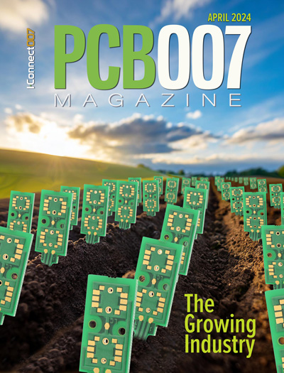
The Growing Industry
In this issue of PCB007 Magazine, we talk with leading economic experts, advocacy specialists in Washington, D.C., and PCB company leadership to get a well-rounded picture of what’s happening in the industry today. Don’t miss it.

The Sustainability Issue
Sustainability is one of the most widely used terms in business today, especially for electronics and manufacturing but what does it mean to you? We explore the environmental, business, and economic impacts.

The Fabricator’s Guide to IPC APEX EXPO
This issue previews many of the important events taking place at this year's show and highlights some changes and opportunities. So, buckle up. We are counting down to IPC APEX EXPO 2024.
- Articles
Article Highlights
- Columns
Search Console
- Links
- Events
||| MENU - pcb007 Magazine
Estimated reading time: 1 minute
Contact Columnist Form
Green Technologies in PCB Fabrication
“Green” and “environmentally friendly” are ill-defined terms. In general, these terms refer to manufacturing that involves the replacement of toxic substances with less toxic materials, the elimination of materials or processing steps, and less consumption of chemicals (i.e., more efficient or higher yield processing, reduction of water use, reduction of energy use, less space requirement, smaller equipment foot print, and recycling and on-site recovery of materials).
Direct Metallization
This family of processes eliminates the electroless copper process. These processes typically have fewer process steps, use less rinse water, have less floor space requirement, and use less toxic chemicals. Direct metallization processes include:
Palladium-based
These processes pretty much follow the classic electroless copper processing step sequence, except the sequence ends with the application of the palladium catalyst, followed by the activation, then skips the electroless bath and proceeds to copper electro-plating.
Carbon or Graphite-based
Using small carbon or graphite particles to render the dielectric hole-wall electro-platable, this process involves very few steps.
Conductive Polymer-based
The process of using a non-conductive monomer to coat the board surface follows an oxidation step that forms a conductive polymer from the non-conductive monomer. The polymer then facilitates copper electro-plating on the non-conductive dielectric hole wall. An example of such a conductive polymer formation is the oxidation of pyrrole to poly-pyrrole, using permanganate as the oxidation agent. The permanganate is reduced to manganese dioxide, which is insoluble and needs to be further reduced to the soluble manganese Mn2+ ion. Another example is the polymerization of “EDOT” (3,4-ethylenedioxy-thiophene) to poly-EDOT.
Read the full column here.
Editor's Note: This column originally appeared in the April 2014 issue of The PCB Magazine.
More Columns from Karl's Tech Talk
Karl's Tech Talk: Digital Imaging UpdateKarl’s Tech Talk: Electronic Packaging Levels
Green Legislation and the Impact on Electronic Materials and Processes
Digital Imaging Revisited
Dry Film Photoresist Thickness Selection Criteria
Quick-Turn Circuit Board Shops
Optical Interconnects
Signal Loss
