-

- News
- Books
Featured Books
- design007 Magazine
Latest Issues
Current Issue
Level Up Your Design Skills
This month, our contributors discuss the PCB design classes available at IPC APEX EXPO 2024. As they explain, these courses cover everything from the basics of design through avoiding over-constraining high-speed boards, and so much more!

Opportunities and Challenges
In this issue, our expert contributors discuss the many opportunities and challenges in the PCB design community, and what can be done to grow the numbers of PCB designers—and design instructors.

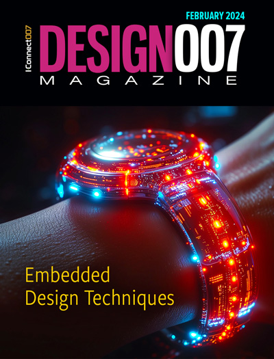
Embedded Design Techniques
Our expert contributors provide the knowledge this month that designers need to be aware of to make intelligent, educated decisions about embedded design. Many design and manufacturing hurdles can trip up designers who are new to this technology.
- Articles
- Columns
Search Console
- Links
- Events
||| MENU - design007 Magazine
Estimated reading time: 1 minute
FAQ - Microwave PCB Materials
The landscape of specialty materials changes so quickly that it can be hard for product developers to keep up. As a result, PCB designers are inundated with data about microwave PCB materials. But very often, it’s difficult to find useful information regarding these specialty substrates. So, this month, we present some of the most frequently asked questions about microwave materials encountered at Rogers.
Q: At what frequency is it necessary to transition from FR-4 types of materials to high-frequency circuit materials?
A: This is a challenging question to answer because different technologies can tolerate more or less performance from a laminate. I’ll give a few examples and basic guidelines.
Semiconductor technology has developed enhanced signal processing to the point where a FR-4 material could be used at higher speeds and frequencies than was once thought possible. In most cases where high-speed digital applications reach 10 Gbps or more, you will need to use a high-frequency laminate. There are exceptions, and in some cases a lower data rate PCB will also demand a high-frequency laminate.
High-frequency RF circuits, which are less concerned with insertion loss, could use FR-4 in some of these applications. However, high-frequency laminates offer more than just low loss; they provide very well-controlled dielectric constant. In many RF applications, the control of dielectric constant for the material can be as critical as substrate thickness control. As a general statement, FR-4 materials are typically not used above 3 GHz in RF applications due to insertion loss concerns. However, when dielectric constant control is a critical concern, high-frequency materials should be used instead of FR-4 materials.
Read the full column here.
Editor's Note: This column originally appeared in the February 2014 issue of The PCB Design Magazine.
More Columns from Lightning Speed Laminates
Lightning Speed Laminates: Millimeter-wave Properties and PCB Design ChallengesLightning Speed Laminates: Optimizing Thermal Management for Wireless Communication Systems
Lightning Speed Laminates: Test Vehicles for PCB Electrical Material Characterization
Lightning Speed Laminates: Optimum Thermal Stability Considerations
Lightning Speed Laminates: Thermal Management Isn’t Getting Easier
Lightning Speed Laminates: Benefits of High-Performance Hybrid Multilayer PCBs
Lightning Speed Laminates: An Overview of Copper Foils
Lightning Speed Laminates: The Importance of Circuit Features for Millimeter-Wave Applications


