


 Marcy's Musings: The Growing Industry
 It’s Only Common Sense: Here’s What To Do After IPC APEX EXPO 2024
 Dan’s Biz Bookshelf: Seeing the How
Ucamco Launches 3 Wavelength Series of Ledia Direct Imaging Systems
September 24, 2015 | UcamcoEstimated reading time: 3 minutes
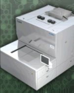
Ucamco is delighted to announce the new 3 Wavelength series of Ledia Direct Imaging (DI) systems for the accurate, high-speed exposure of the industry's most demanding soldermask, inner-layer and outer-layer resists.
When it comes to the direct imaging of PCB materials, Dai Nippon Screen's Ledia multi-wavelength UV LED DI platform has always led the field. First, with its 2 Wavelength Ledia imaging systems, Screen delivered unprecedented DI throughputs on even the most demanding inner- and outer-layer resists, and it gave PCB manufacturers the very first DI technology with which to process standard soldermask resists accurately and at production speeds.
Now, building on that success, Ucamco is launching Screen's 3 Wavelength series. These 5 and 6 exposure head systems combine optimised 365, 385 and 405nm wavelength LED emissions into the industry's most powerful DI system to date. With it, even the most difficult soldermasks can be imaged accurately and reliably, at up to twice previous speeds, with excellent solder dam edge quality, and no undercut. Even when processing inner- and outer-layers, Ledia's new systems deliver more: ultrafine 15µm lines and spaces with well-defined edges, and significant improvements in throughput.
Direct Imaging makes a whole lot of sense at a time when PCBs are getting smaller and increasingly densely packed with tiny components and features. Conventional exposure methods just can't keep up – phototool films move with changes in temperature and humidity, and as the boards get smaller and the work becomes finer, getting it right becomes increasingly time-consuming, if not impossible, making registration the biggest bottleneck for many PCB manufacturers, and the source of some very expensive scrap.
Ledia eliminates the problems by handling each board on its own merits, independent of feature size, board size or production volumes, says Ucamco's Imaging Group Director Michel Van den Heuvel: “We see Ledia as a registration machine – with its inbuilt real-time positioning system and Screen's proprietary alignment algorithms, it automatically registers each board to within a few microns, cutting valuable seconds, and even in some rare cases, many minutes, off the exposure time for each board or panel”.
Ledia's soldermask capabilities put it in a class of its own, and accordingly, sales are growing fast, as Van den Heuvel explains: “At first, manufacturers could not believe that standard soldermask could be processed with DI technology with the speeds and quality that are essential to our industry. This is because it is less photosensitive than dry film resists, and coating thickness can be variable, making it difficult to expose uniformly from the top to the bottom of the resist. But as we started to place our multiwavelength systems with pioneering PCB makers, news travelled, and sales have taken off”. Indeed, the ultimate drop-in technology, Ledia improves quality, yields and leadtimes. And yet it is more economical to run, and its light sources last longer and are less expensive than those used by other exposure processes.
In short, it's light years ahead of other PCB imaging systems – and thanks to the new 3 Wavelength series, it looks set to stay there, delivering significant improvements in terms of quality, productivity and yields – all of which directly impact the bottom line. Which is why Europe's most successful PCB manufacturers are turning to Ledia.
Why not join them? Contact Ucamco today and find out how Ledia can boost your business.
About Ucamco
Ucamco (formerly Barco ETS) is a market leader in PCB CAM software, photoplotting and direct imaging systems, with a global network of sales and support centers. Headquartered in Ghent, Belgium, Ucamco has over 25 years of ongoing experience in developing and supporting leading-edge photoplotters and front-end tooling solutions for the global PCB industry. Key to this success is the company's uncompromising pursuit of engineering excellence in all its products.
Share on:


Suggested Items
AIM to Highlight NC259FPA Ultrafine No Clean Solder Paste at SMTA Wisconsin Expo & Tech Forum
04/18/2024 | AIMAIM Solder, a leading global manufacturer of solder assembly materials for the electronics industry, is pleased to announce its participation in the upcoming SMTA Wisconsin Expo & Tech Forum taking place on May 7 at the Four Points by Sheraton | Milwaukee Airport, in Milwaukee, Wisconsin.
Hentec/RPS Publishes an Essential Guide to Selective Soldering Processing Tech Paper
04/17/2024 | Hentec Industries/RPS AutomationHentec Industries/RPS Automation, a leading manufacturer of selective soldering, lead tinning and solderability test equipment, announces that it has published a technical paper describing the critical process parameters that need to be optimized to ensure optimal results and guarantee the utmost in end-product quality.
Empowering Electronics Assembly: Introducing ALPHA Innolot MXE Alloy
04/16/2024 | MacDermid Alpha Electronics SolutionsIn the rapidly evolving electronics industry, where innovation drives progress, MacDermid Alpha Electronics Solutions is committed to setting a new standard. Today, we are pleased to introduce ALPHA Innolot MXE, a revolutionary alloy meticulously engineered to address the critical needs of enhanced reliability and performance in modern electronic assemblies.
New Book on Low-temperature Soldering Now Available
04/17/2024 | I-Connect007I-Connect007 is pleased to announce that The Printed Circuit Assembler’s Guide to… Low-temperature Soldering, Vol. 2, by subject matter experts at MacDermid Alpha Electronics Solutions, is now available for download.
Inkjet Solder Mask ‘Has Arrived’
04/10/2024 | Pete Starkey, I-Connect007I was delighted to be invited to attend an interactive webinar entitled “Solder Mask Coating Made Easy with Additive Manufacturing,” hosted by SUSS MicroTec Netherlands in Eindhoven. The webinar was introduced and moderated by André Bodegom, managing director at Adeon Technologies, and the speakers were Mariana Van Dam, senior product manager PCB imaging solutions at AGFA in Belgium; Ashley Steers, sales manager at Electra Polymers in the UK; and Dr. Luca Gautero, product manager at SUSS MicroTec Netherlands.