


 Marcy's Musings: The Growing Industry
 It’s Only Common Sense: Here’s What To Do After IPC APEX EXPO 2024
 Dan’s Biz Bookshelf: Seeing the How
All About Flex: Process Controls for Flexible Circuit Fabrication
December 17, 2015 | Dave Becker, All FlexEstimated reading time: 1 minute
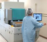
Manufacturers of flexible circuits use several chemical processes for fabrication. These processes are generally located in a common area of the plant because of facility requirements and environmental considerations. These chemical operations are referred to as wet processes. Some of the specific processes that would be characterized as wet process in circuit fabrication:
• Develop-etch-strip: Photosensitive resist is developed so the unneeded resist is washed away, leaving a pattern of resist that defines the circuitry. The subsequent etching operation removes the base metal (normally copper) that has been exposed by the patterned resist. The last step is to remove (strip away) the resist that defined the circuitry.
• Copper plating: This is typically an electro-chemical operation. Metal is electrodeposited onto the base metal surface thereby creating a thin, robust coating. Electroplating of copper is the most common example and is used to create electrical connection between traces on the top and bottom of the insulating dielectric film.
• Shadow plating: A laminate of metal-dielectric-metal is initially drilled, punched, or laser ablated to form the vias. In order to initially create an electrical connection between the layers of metal, the dielectric must be coated with a conductive material. Shadow plating coats graphite inside a via and is a chemical process commonly used by flexible circuit manufacturers.
Each of these operations relies on chemical reactions, which may be supplemented with mechanical agitation, temperature and voltage/current. In most cases the chemical makeup is the most critical element that affects the output. It is vital that critical process parameters are tightly controlled to assure desired results. The following are the basic outputs that are monitored and compared to a process or customer specification:
- Trace width and spacing
- Metal thickness
- Via integrity
- Metal composition
To read the full article click here.
Editor's Note: This article originally appeared in the November 2015 issue of The PCB Magazine.
Share on:


Suggested Items
Insulectro’s 'Storekeepers' Extend Their Welcome to Technology Village at IPC APEX EXPO
04/03/2024 | InsulectroInsulectro, the largest distributor of materials for use in the manufacture of PCBs and printed electronics, welcomes attendees to its TECHNOLOGY VILLAGE during this year’s IPC APEX EXPO at the Anaheim Convention Center, April 9-11, 2024.
ENNOVI Introduces a New Flexible Circuit Production Process for Low Voltage Connectivity in EV Battery Cell Contacting Systems
04/03/2024 | PRNewswireENNOVI, a mobility electrification solutions partner, introduces a more advanced and sustainable way of producing flexible circuits for low voltage signals in electric vehicle (EV) battery cell contacting systems.
Heavy Copper PCBs: Bridging the Gap Between Design and Fabrication, Part 1
04/01/2024 | Yash Sutariya, Saturn Electronics ServicesThey call me Sparky. This is due to my talent for getting shocked by a variety of voltages and because I cannot seem to keep my hands out of power control cabinets. While I do not have the time to throw the knife switch to the off position, that doesn’t stop me from sticking screwdrivers into the fuse boxes. In all honesty, I’m lucky to be alive. Fortunately, I also have a talent for building high-voltage heavy copper circuit boards. Since this is where I spend most of my time, I can guide you through some potential design for manufacturability (DFM) hazards you may encounter with heavy copper design.
Trouble in Your Tank: Supporting IC Substrates and Advanced Packaging, Part 5
03/19/2024 | Michael Carano -- Column: Trouble in Your TankDirect metallization systems based on conductive graphite or carbon dispersion are quickly gaining acceptance worldwide. Indeed, the environmental and productivity gains one can achieve with these processes are outstanding. In today’s highly competitive and litigious environment, direct metallization reduces costs associated with compliance, waste treatment, and legal issues related to chemical exposure. What makes these processes leaders in the direct metallization space?
AT&S Shines with Purest Copper on World Recycling Day
03/18/2024 | AT&SThe Styrian microelectronics specialist AT&S is taking World Recycling Day as an opportunity to review the progress that has been made in recent months at its sites around the world in terms of the efficient use of resources: