


 It’s Only Common Sense: OCCAM—the Time Is Now
 Marcy's Musings: The Growing Industry
 Dan’s Biz Bookshelf: Seeing the How
New Material and Process Solutions for the Electronic Interconnection Industry
February 26, 2016 | Joseph Fjelstad, Verdant ElectronicsEstimated reading time: 1 minute
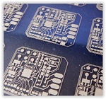
Introduction
The manufacture of electronics has, for the last several decades, followed a production script that has changed little over time. The vast majority of printed circuits are still being manufactured and assembled using materials and processes that the pioneers of the early printed circuit industry would easily recognize. The primary reason is that most circuit design practices are deeply rooted and tied to traditional manufacturing methods. However, these methods are not the only ones that can be used to manufacture and assemble printed circuits today. In fact, it is arguable that traditional methods are not as well-suited to the manufacture of today’s more challenging product designs. This is a fact that has not been lost on Japanese product engineers. Over the last nearly two decades, they have conceived of and reduced to practice a number of unique methods for making high-density interconnection product. One of the important keys to making this possible has been the development of materials uniquely designed and structured to filling special needs of these advanced circuit designs.
Though perhaps not a household name, 70-year-old Tatsuta Electric Wire & Cable Co., Ltd. has been at the forefront of the development of such materials for many years. As the name implies, the company was originally focused on providing wire and cabling solutions for the electrical and electronics industries. However, realizing that the scope of their business extended beyond wire harnesses and cables, the company began to develop materials suited to the needs of printed wiring manufacturers and assemblers. This article has been prepared to familiarize the readers of this esteemed electronics publication of some of the new material and process solutions the company has developed and is making available to the industry.
Editor's Note: This article originally appeared in the February 2016 issue of The PCB Magazine
Share on:


Suggested Items
Winner of The Science Show Rakett 69 Receives Incap Scholarship
04/24/2024 | IncapThe winner of the Rakett 69 science show, Andri Türkson, who stood out as an electronics enthusiast, received a scholarship from Incap Estonia, along with an internship opportunity in Saaremaa.
Alternative Manufacturing Inc. Awarded QML Requalification to IPC J-STD-001 and IPC-A-610
04/24/2024 | IPCIPC's Validation Services Program has awarded an IPC J-STD-001 and IPC-A-610 Qualified Manufacturers Listing (QML) requalification to Alternative Manufacturing Inc (AMI).
Boeing's Janene Stinson Earns IPC Excellence in Education Award at IPC APEX EXPO 2024
04/22/2024 | IPCThe IPC Excellence in Education award was presented to Janene Stinson, Boeing, at IPC APEX EXPO 2024 in Anaheim, California, in recognition of her significant contributions to workforce development and leadership.
Zentech’s Board of Directors Announces the Return of Matt Turpin as President and CEO
04/22/2024 | Zentech ManufacturingTurpin draws upon over 35 years of experience in the electronics industry and has an 18-year history with Zentech. He previously served as President and CEO from 2006 to 2019 after which time he has remained active in the EMS industry as an advisor to Zentech and other industry organizations.
IDTechEx Report Unveils 3D Electronics Status and Opportunities
04/22/2024 | PRNewswire3D electronics is an emerging manufacturing approach that enables electronics to be integrated within or onto the surface of objects. 3D electronic manufacturing techniques empower new features, including mass customizability, greater integration, and improved sustainability in the electronics industry.