-

- News
- Books
Featured Books
- pcb007 Magazine
Latest Issues
Current Issue
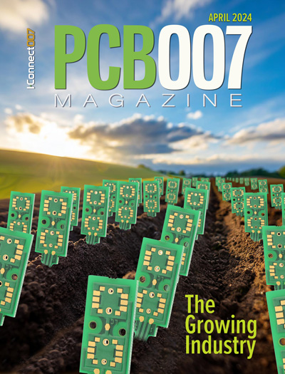
The Growing Industry
In this issue of PCB007 Magazine, we talk with leading economic experts, advocacy specialists in Washington, D.C., and PCB company leadership to get a well-rounded picture of what’s happening in the industry today. Don’t miss it.

The Sustainability Issue
Sustainability is one of the most widely used terms in business today, especially for electronics and manufacturing but what does it mean to you? We explore the environmental, business, and economic impacts.

The Fabricator’s Guide to IPC APEX EXPO
This issue previews many of the important events taking place at this year's show and highlights some changes and opportunities. So, buckle up. We are counting down to IPC APEX EXPO 2024.
- Articles
- Columns
Search Console
- Links
- Events
||| MENU - pcb007 Magazine
The Sum of All Parts: Planning for a First-Time-Right PCB Design
May 17, 2016 | Sam Sangani, PNC Inc.Estimated reading time: 2 minutes
The development of highly integrated and high-speed, chip-based circuit boards brings several functional benefits. But at the same time, these can introduce additional challenges to the actual board itself. Therefore, developing an effective plan for designing, developing, testing and producing the final PCBs is a good business practice.
Lack of communication between PCB designers and PCB fabricators is one of the most significant issues we have faced in our industry. This has led to disconnect in the mutual understanding between these two entities. Subsequently, a scenario has arisen where manufacturers lack the understanding of design guidelines and some designers are not always aware of the manufacturing processes and capabilities of a PCB manufacturer during their design/layout phase.
If we are going to succeed—particularly at the domestic level—we need to open up channels of communication.
Several steps in the PCB design and manufacturing process include areas that allow enhancements that would improve the ease with which boards can be manufactured and decrease the loss rate. Many elements of the process, from the design process to final board test, should be reviewed for improvements that can affect the board’s manufacturability. The ideal way to negate the aforementioned drawbacks would be to design and produce under one roof but, until such a time where this is possible on a large scale, certain measures can be taken to optimize the process as much as possible.
Here are five reasons why designers and PCB manufacturers need to communicate:
1. Critical tolerances vs. yield
With regard to determining what the process can and cannot do, this is a very important factor which affects yield and cost associated in PCB manufacturing.
2. Component placement and solderability
A variation in component density over a PCB surface impacts the uniformity of the soldering of components. Very dense areas may not get enough heat during the reflow process and could result in cold solder joints.
3. Size and uniformity
As the surface area of a PCB gets larger, it brings unwanted irregularities in manufacturing such as the registration of via to pad and warpage on the board surface, making SMT pads or BGA balls unconnected to the PCB. If the proper thickness and stack-up design are taken into account in the initial stages, it would help resolve these types of issues earlier.
4. Transparency
Designers and fabricators working side by side on R&D projects opens up doors not only for the parties involved, but also makes an overall contribution to the industry. Stay up-to-date on new development in processes and technologies. The industry—especially now—is changing rapidly.
5. Long-term business relationships
Once a designer and the PCB manufacturer are actively engaged and get know each other, designers are less likely to try to switch PCB suppliers and start building their relations from scratch. Instead, they can keep building better products when they better understand each other.
Fortunately, communications are moving in the right direction. More and more designers and board houses are starting to engage in productive discussions. Designers are reaching out for plant tours and are developing an interest in the manufacturing process. Golden advice to designers: Do not miss open houses and seminars organized by PCB vendors. Golden advice to PCB suppliers: Do your best to understand designers’ needs.
Sam Sangani is president and CEO of PNC Inc.
Suggested Items
Taiyo Circuit Automation Installs New DP3500 into Fuba Printed Circuits, Tunisia
04/25/2024 | Taiyo Circuit AutomationTaiyo Circuit Automation are proud to be partnered with Fuba Printed Circuits, Tunisia part of the OneTech Group of companies, a leading printed circuit board manufacturer based out of Bizerte, Tunisia. on their first installation of Taiyo Circuit Automation DP3500 coater.
Vicor Power Orders Hentec Industries/RPS Automation Pulsar Solderability Testing System
04/24/2024 | Hentec Industries/RPS AutomationHentec Industries/RPS Automation, a leading manufacturer of selective soldering, lead tinning and solderability test equipment, is pleased to announce that Vicor Power has finalized the purchase of a Pulsar solderability testing system.
AIM Solder’s Dillon Zhu to Present on Ultraminiature Soldering at SMTA China East
04/22/2024 | AIMAIM Solder, a leading global manufacturer of solder assembly materials for the electronics industry, is pleased to announce that Dillon Zhu will present on the topic: Ultraminiature Soldering: Techniques, Technologies, and Standards at SMTA China East. This event is being held at the Shanghai World Expo Exhibition & Convention Center from April 24-25.
AIM to Highlight NC259FPA Ultrafine No Clean Solder Paste at SMTA Wisconsin Expo & Tech Forum
04/18/2024 | AIMAIM Solder, a leading global manufacturer of solder assembly materials for the electronics industry, is pleased to announce its participation in the upcoming SMTA Wisconsin Expo & Tech Forum taking place on May 7 at the Four Points by Sheraton | Milwaukee Airport, in Milwaukee, Wisconsin.
Hentec/RPS Publishes an Essential Guide to Selective Soldering Processing Tech Paper
04/17/2024 | Hentec Industries/RPS AutomationHentec Industries/RPS Automation, a leading manufacturer of selective soldering, lead tinning and solderability test equipment, announces that it has published a technical paper describing the critical process parameters that need to be optimized to ensure optimal results and guarantee the utmost in end-product quality.


