


 Marcy's Musings: The Growing Industry
 It’s Only Common Sense: Here’s What To Do After IPC APEX EXPO 2024
 Dan’s Biz Bookshelf: Seeing the How
LDS MIDs: Ready for the Next Generation in Wireless Technology
May 30, 2016 | LPKFEstimated reading time: 2 minutes
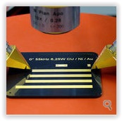
As frequency increases, so do the demands on antenna components. In cooperation with the Institute of High Frequency Technology and Radio Systems (Institut für Hochfrequenztechnik und Funksysteme, HFT) at Leibniz University of Hannover, the LPKF LDS technique is currently being scrutinized for its suitability for next-generation wireless applications.
Publications due for release in late mid-2016 demonstrate the applicability of the LDS technology for antennas in the millimeter-wave frequency band - for example, for fifth-generation (5G) wireless technology or for automotive sensors.
Challenging demands accompanied by increasing device densities and extension of frequency bands mean that flexible approaches are needed to functionalize existing installation space for high-frequency applications. MID technology represents a solution. It allows electrical structures, such as antennas, to be applied to nearly any surface.
Dipl.-Ing. Aline Friedrich, a PhD student at HFT, has worked with 3D-MID technologies for many years: “Three-dimensional antennas offer huge advantages for certain applications. It has already been shown with prototypes that, with the proper layout, three-dimensional antennas represent a powerful alternative to conventional configurations.” The three-dimensional design allows for flexible antenna development so that solutions can be found to meet even the most challenging demands of the future.
HFT uses Laser Direct Structuring (LDS) technology in its development work. With LDS, a laser beam structures a three-dimensional part made of an LDS-doped plastic. The laser beam transfers the desired circuit layout onto the substrate while activating the additive at the same time. In a subsequent electroless metallization step, copper layers are built up on the structures traversed by the laser beam. These layers can then be given various surface finishes.
LDS technology is already established as a preferred manufacturing tech-nique for three-dimensional antennas in the consumer goods sector. LDS antennas covering the frequency band up to 6 GHz, e.g., for Bluetooth, LTE, or Wi-Fi, can be found in many of today’s smartphones, tablets, and wearable devices.
The higher the transmission frequency, the shorter the wavelength - and the greater the demands on the components. The question as to the relevant manufacturing criteria for RF applications beyond 6 GHz formed the basis for the cooperation between HFT and LPKF.
Because next-generation wireless systems for consumer electronics and smart homes are also expected to see an extension of the operating frequency bands to include higher frequencies, one focus of the cooperation is on evaluation and optimization of LDS production for applications in the millimeter-wave frequency band, e.g., for 5G communications technologies. The first prototypes of an antenna for use in millimeter-wave sensors operating at 24 GHz were produced at HFT and measurements verified its success. Production of test antennas operating at 77 GHz is currently underway. The results of the test measurements are also extremely promising for these applications and demonstrate the potential for LDS-based antennas operating at higher frequencies.
Technical papers are expected to be published in late summer 2016. Re-sults will then be discussed through scientific journals and international conferences. Further information can be obtained from Malte Fengler, Product Manager at LPKF.
Share on:


Suggested Items
Insulectro’s 'Storekeepers' Extend Their Welcome to Technology Village at IPC APEX EXPO
04/03/2024 | InsulectroInsulectro, the largest distributor of materials for use in the manufacture of PCBs and printed electronics, welcomes attendees to its TECHNOLOGY VILLAGE during this year’s IPC APEX EXPO at the Anaheim Convention Center, April 9-11, 2024.
ENNOVI Introduces a New Flexible Circuit Production Process for Low Voltage Connectivity in EV Battery Cell Contacting Systems
04/03/2024 | PRNewswireENNOVI, a mobility electrification solutions partner, introduces a more advanced and sustainable way of producing flexible circuits for low voltage signals in electric vehicle (EV) battery cell contacting systems.
Heavy Copper PCBs: Bridging the Gap Between Design and Fabrication, Part 1
04/01/2024 | Yash Sutariya, Saturn Electronics ServicesThey call me Sparky. This is due to my talent for getting shocked by a variety of voltages and because I cannot seem to keep my hands out of power control cabinets. While I do not have the time to throw the knife switch to the off position, that doesn’t stop me from sticking screwdrivers into the fuse boxes. In all honesty, I’m lucky to be alive. Fortunately, I also have a talent for building high-voltage heavy copper circuit boards. Since this is where I spend most of my time, I can guide you through some potential design for manufacturability (DFM) hazards you may encounter with heavy copper design.
Trouble in Your Tank: Supporting IC Substrates and Advanced Packaging, Part 5
03/19/2024 | Michael Carano -- Column: Trouble in Your TankDirect metallization systems based on conductive graphite or carbon dispersion are quickly gaining acceptance worldwide. Indeed, the environmental and productivity gains one can achieve with these processes are outstanding. In today’s highly competitive and litigious environment, direct metallization reduces costs associated with compliance, waste treatment, and legal issues related to chemical exposure. What makes these processes leaders in the direct metallization space?
AT&S Shines with Purest Copper on World Recycling Day
03/18/2024 | AT&SThe Styrian microelectronics specialist AT&S is taking World Recycling Day as an opportunity to review the progress that has been made in recent months at its sites around the world in terms of the efficient use of resources:
Copyright © 2024 I-Connect007 | IPC Publishing Group Inc. All rights reserved.
Log in