


 Material Insight: The Dielectric Constant of PCB Materials
 American Made Advocacy: What About the Rest of the Technology Stack?
 It’s Only Common Sense: Great Ideas From John Mitchell’s Book on Hiring Habits
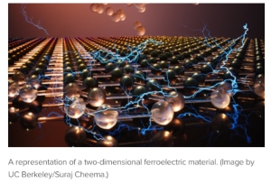
Thinnest Ferroelectric Material Ever Paves the Way for New Energy-efficient Devices
October 21, 2022 | Argonne National LaboratoryEstimated reading time: 3 minutes
As electronic devices become smaller and smaller, the materials that power them need to become thinner and thinner. Because of this, one of the key challenges scientists face in developing next-generation energy-efficient electronics is discovering materials that can maintain special electronic properties at an ultrathin size.
Advanced materials known as ferroelectrics present a promising solution to help lower the power consumed by the ultrasmall electronic devices found in cell phones and computers. Ferroelectrics — the electrical analog to ferromagnets — are a class of materials in which some of the atoms are arranged off-center, leading to a spontaneous internal electric charge or polarization. This internal polarization can reverse its direction when scientists expose the material to an external voltage. This offers great promise for ultralow-power microelectronics.
Unfortunately, conventional ferroelectric materials lose their internal polarization below around a few nanometers in thickness. This means they are not compatible with current-day silicon technology. This issue has previously prevented the integration of ferroelectrics into microelectronics.
But now a team of researchers from the University of California at Berkeley performing experiments at the U.S.
Department of Energy’s (DOE) Argonne National Laboratory have found a solution that simultaneously solves both problems by creating the thinnest ferroelectric ever reported and the thinnest demonstration of a working memory on silicon.
In a study published in the journal Science, the research team discovered stable ferroelectricity in an ultrathin layer of zirconium dioxide just half a nanometer thick. That’s the size of a single atomic building block, about 200,000 times thinner than a human hair. The team grew this material directly on silicon. They found ferroelectricity emerges in zirconium dioxide — normally a nonferroelectric material — when it is grown extremely thin, approximately 1-2 nanometers in thickness.
Notably, the ferroelectric behavior continues to its near-atomic-scale thickness limit of roughly half a nanometer. This fundamental breakthrough marks the world’s thinnest ferroelectric. This is surprising for a material that is not even typically ferroelectric in its bulk form.
The researchers were also able to switch the polarization in this ultrathin material back and forth with a small voltage, enabling the thinnest demonstration of a working memory ever reported on silicon. It also offers substantial promise for energy-efficient electronics, especially considering conventional zirconium dioxide is already present in today’s state-of-the-art silicon chips.
“This work takes a key step towards integrating ferroelectrics into highly scaled microelectronics,” said Suraj Cheema, a postdoctoral researcher at UC Berkeley, the first author of the study.
Visualizing the ferroelectric behavior of such ultrathin systems required the use of Argonne’s Advanced Photon Source, a DOE Office of Science user facility. ?“X-ray diffraction gives needed insight into how this ferroelectricity emerges,” said Argonne physicist John Freeland, another author of the study.
Beyond the immediate technological impact, this work also has significant implications for designing new two-dimensional materials.
“Simply squeezing 3D materials to their 2D thickness limit offers a straightforward-yet-effective route to unlocking hidden phenomena in a wide variety of simple materials,” Cheema said. ?“This greatly expands the materials design space for next-generation electronics to include materials already compatible with silicon technologies.”
As Cheema noted, simply growing just a few atomic layers of a 3D material can offer the potential for a new class of 2D materials — atomically-thin 3D materials — that go beyond conventional sheets of 2D materials like graphene. The researchers hope this work will motivate more research into two-dimensional 3D materials exhibiting emergent electronic phenomena relevant for energy-efficient electronics.
This work was led by Cheema and Sayeef Salahuddin of UC Berkeley, along with co-first authors Nirmaan Shanker and Shang-Lin Hsu. At beamline 33-BM-C of Argonne’s Advanced Photon Source, working with Argonne physicists Freeland and Zhan Zhang, the researchers employed synchrotron X-ray absorption spectroscopy and X-ray diffraction to investigate the structural evolution of ferroelectricity to the atomic scale and explore its electronic origins. At DOE’s Lawrence Berkeley National Laboratory’s Advanced Light Source and Molecular Foundry, collaborating with scientists Padraic Shafer and Jim Ciston, the material’s ferroelectric crystal structure was studied using soft X-rays and transmission electron microscopy.
Share on:


Suggested Items
Material Insight: The Dielectric Constant of PCB Materials
05/17/2024 | Dr. Preeya Kuray -- Column: Material InsightIn the world of PCB design, miniaturization can be achieved by using low dielectric constant (Dk) materials. Low Dk materials can allow for a reduction in thickness while maintaining a given trace width, leading to lower transmission loss and higher density circuitry.
IPC APEX EXPO: Some Thoughts About Growth
05/16/2024 | Dan Feinberg, I-Connect007After two and a half days of wandering the aisles at IPC APEX EXPO 2024, for the first time, I almost felt like I was exploring CES. There were so many booths and exhibits that I could describe, but I’d like to focus on the growth and huge value of this event, which has expanded well beyond just the growing and impressive exhibit show floor.
The Shaughnessy Report: Unlock Your High-speed Material Constraints
05/15/2024 | Andy Shaughnessy -- Column: The Shaughnessy ReportThe world of PCB materials used to be a fairly simple one. It was divided into two groups: the “traditional” laminates, often called FR-4, and the high-speed laminates developed especially for high-speed PCBs. These were two worlds that usually didn’t collide. But then traditional laminates started getting better, and high-speed designers and design engineers took notice and started to reconsider what FR-4 could be used for.
Breaking High-speed Material Constraints: Design007 Magazine — May 2024
05/14/2024 | I-Connect007 Editorial TeamDo you need specialty materials for your high-speed designs? Maybe not. Improvements in resins mean designers of high-speed boards can sometimes use traditional laminate systems instead of high-speed materials, saving time and money while streamlining the fab process. In the May 2024 issue of Design007 Magazine, our contributors explain how to avoid overconstraining your materials when working with high-speed boards.
Indium Experts to Present at Electronics in Harsh Environments SMTA Conference
05/13/2024 | Indium Corporationndium Corporation Technical Manager for Europe, Africa, and the Middle East, Karthik Vijay, will deliver a technical presentation and Indium Corporation Senior Technologist, Dr. Ronald Lasky, will deliver both a workshop and technical presentation at the Electronics in Harsh Environments SMTA Conference on May 14-16 in Copenhagen, Denmark.