


 Material Insight: The Dielectric Constant of PCB Materials
 American Made Advocacy: What About the Rest of the Technology Stack?
 It’s Only Common Sense: Great Ideas From John Mitchell’s Book on Hiring Habits
ITRI Announces Collaborates with K&S in Hi-CHIP Alliance
November 29, 2022 | ITRIEstimated reading time: 2 minutes
ITRI welcomes Kulicke and Soffa Industries, Inc. (K&S) to the Heterogeneous Integration and Chip-let System Package (Hi-CHIP) Alliance, an initiative launched by ITRI in 2021. K&S is one of the world’s largest semiconductor packaging and electronic assembly solution providers. With the participation of K&S, the Alliance is expected to join hands with supply chain players to strengthen the process capability of the chip industry and create cutting-edge advantages in the global market.
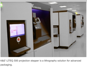
The Hi-CHIP Alliance leverages K&S’s advanced packaging competencies and its LITEQ 500 lithography process to address emerging challenges within the redistribution layer (RDL) forming process. High-density RDL is an enabler for high-density fan-out wafer-level packaging (HD FOWLP) and similar approaches which provide performance, thermal management, power consumption and form-factor improvements, benefiting broad applications in major markets including the telecommunications, computing, automotive, and biomedical markets.
In addition to providing a market-ready solution for emerging heterogenous applications, high-density RDL processing is also utilized within many other fast-growing applications, including Antenna-in-Package for 5G mmWave and sub-6 GHz RF modules, integrated solutions for baseband and smartphone application processors, artificial intelligence solutions integrated with RF and memory, and transistor-dense applications such as System in Packages. These emerging applications are anticipated to outpace broader integrated circuit growth by demanding new RDL solutions which the LITEQ 500 can address.
K&S’ LITEQ 500 lithography projection stepper uses a laser-based light source to provide high-intensity exposures without intensity degradation over time. This approach delivers high throughput, long lifetime, high uptime, and low cost of ownership. The single-wavelength light source enables the use of high-transmission and low-aberration optics, which makes it a compelling choice for high-density RDL applications.
Dr. Shih-Chieh Chang, General Director of ITRI’s Electronic and Optoelectronic System Research Laboratories, expressed his excitement to have K&S on board with the Hi-CHIP Alliance. As K&S has been known as an industry leading company, he believes that this partnership can further explore process and equipment solutions for future packaging and assembly challenges. “K&S as an industry leader and pioneer helps further explore future semiconductor assembly processes and solutions,” he added. With the support from the Department of Technology, Ministry of Economic Affairs, ITRI has been innovating semiconductor technologies and will continue to develop world-leading technologies as a bellwether for the semiconductor industry.
“We are delighted to collaborate with ITRI on next-generation applications. This offers a unique opportunity to further enable the adoption and extend the value of our growing advanced packaging portfolio,” said Joeri Durinckx, K&S’ Vice President for EA/APMR & Lithography Business Units.
Share on:


Suggested Items
Avnet Launches QCS6490 Vision-AI Development Kit
05/17/2024 | AvnetThe QCS6490 Vision-AI Development Kit from Avnet enables engineering teams to rapidly prototype hardware, application software and AI enablement for multi-camera, high-performance, Edge AI-enabled custom embedded products.
Standard of Excellence: Collaboration—The Right Path to Innovation
05/15/2024 | Anaya Vardya -- Column: Standard of ExcellenceNow more than ever, as new and innovative technologies for printed circuit boards are in demand, we need collaboration between PCB designers, fabricators, and assemblers. Close partnerships with PCB designers and assemblers are key to developing and producing PCBs with boards with new and innovative technology. These collaborative partnerships, along with the partnership with the end customers, are more critical than ever before.
Listen Up: Popular Podcast Series Returns With Discussion of Electroless Copper
05/16/2024 | I-Connect007In the latest episode of the podcast series, On the Line With: Designing for Reality, Nolan Johnson returns to Sunstone Circuits in Mulino, OR, to continue down the manufacturing process with Matt Stevenson.
Breaking High-speed Material Constraints: Design007 Magazine — May 2024
05/14/2024 | I-Connect007 Editorial TeamDo you need specialty materials for your high-speed designs? Maybe not. Improvements in resins mean designers of high-speed boards can sometimes use traditional laminate systems instead of high-speed materials, saving time and money while streamlining the fab process. In the May 2024 issue of Design007 Magazine, our contributors explain how to avoid overconstraining your materials when working with high-speed boards.
IDENTCO Highlights Automation Capabilities and PCB Labeling at PCB East
05/13/2024 | IDENTCOIDENTCO – a manufacturer of high-performance labeling solutions for the power equipment, electronics, transportation, and general industrial sector – will highlight its automation capabilities and PCB labeling solutions at PCB East, June 4-7 in Boxborough, MA, Booth #301.