


 It’s Only Common Sense: OCCAM—the Time Is Now
 Marcy's Musings: The Growing Industry
 Dan’s Biz Bookshelf: Seeing the How
Innovative Electroplating Processes for IC Substrates
August 27, 2019 | S. Dharmarathna, S. Maddux, C. Benjamin, I. Li, W. Bowerman, K. Feng, and J. Watkowski, MacDermid Alpha Electronics SolutionsEstimated reading time: 3 minutes
Abstract
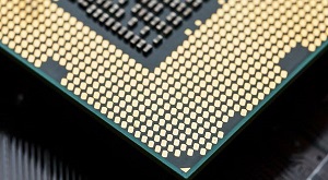
In this era of electronics miniaturization, high-yield and low-cost integrated circuit (IC) substrates play a crucial role by providing a reliable method of high-density interconnection (HDI) of the chip to the board. To maximize substrate real estate, the distance between copper traces—also known as line and space (L/S)- should be minimized. Typical PCB technology consists of L/S larger than 40 µm whereas more advanced wafer-level technology currently sits at or around 2 µm L/S. In the past decade, the chip size has decreased significantly along with the L/S on the substrate. The decreasing chip scales and smaller L/S distances have created unique challenges for both the printed circuit board (PCB) industry and the semiconductor industry.
Fan-out panel-level packaging (FOPLP) is a new manufacturing technology that seeks to bring the PCB world and IC/semiconductor world even closer. While FOPLP is still an emerging technology, the amount of high-volume production in this market space provide a financial incentive to develop innovative solutions to enable its ramp-up. The most important performance aspect of the fine-line plating in this market space is plating uniformity or planarity. Plating uniformity, trace/via top planarity (which measures how flat the top of the traces), and vias are a few major features. This is especially important in multilayer processing, as nonuniformity on a lower layer can be transferred to successive layers, disrupting the device design with catastrophic consequences, such as short circuits. Additionally, a non-planar surface could also result in signal transmission loss by distortion of the connecting points (i.e., vias and traces). Therefore, plating solutions that provide a uniform, planar profile without any special post-treatment are quite desirable.
Here, we discuss innovative additive packages for direct-current copper electroplating specifically for IC substrates with capabilities such as embedded trench fill and simultaneous through-hole plating and via filling with an enhanced pattern plate. These new solutions not only offer better trace profile, but they also deliver via fill and through-hole plating. We also describe two electrolytic copper plating processes, the selection of which could be based on the via size and the dimple requirements of the application. Process I offers great via fill for deeper vias up to 80–120 µm diameter and 50–100µm deep. Process II is more suitable for shallow smaller vias 50–75 µm diameter and 30–50 µm deep.
In this article, we show that these two processes provide excellent surface uniformity and trace profile while also providing via filling and through-hole plating capabilities when controlled within given parameters. Process optimization and thermal and physical characterization of the metallization are also presented.
Introduction
The IC substrate is the highest level of miniaturization in PCB technology, providing the connection between the IC chip and the PCB. These connections are created through a network of electrically conductive copper traces and through-holes. The density of the traces is a crucial factor in terms of miniaturization, speed, and portability of consumer electronics. Trace density has grown immensely over the past few decades to meet today’s printed circuit designs, which include thin core material, fine-line widths, and smaller diameter through-holes and blind vias. The development of fan-out panel-level packaging (FOPLP) has been a topic among the microelectronics community for some time.
The main driving forces to push this new technology are cost and productivity. Traditional fan-out wafer-level packaging (FOWLP) uses a 300-mm wafer as the production vehicle because larger wafers are difficult to obtain. Therefore, the FOWLP has a limitation on the basic unit of process, thereby increasing the processing steps, manpower, and cost while also having a low yield. The advantage of using a PCB-like substrate is that manufacturers have more design flexibility and surface area compared to the wafer. As an example, a 610 x 457 mm panel has almost four times the surface area of a 300-mm wafer. Therefore, processing a panel this size drastically reduces cost, time, and processing steps. This is a huge advantage for the high-volume production market.
To read the full article, which appeared in the August 2019 issue of PCB007 Magazine, click here.
Share on:


Suggested Items
Insulectro’s 'Storekeepers' Extend Their Welcome to Technology Village at IPC APEX EXPO
04/03/2024 | InsulectroInsulectro, the largest distributor of materials for use in the manufacture of PCBs and printed electronics, welcomes attendees to its TECHNOLOGY VILLAGE during this year’s IPC APEX EXPO at the Anaheim Convention Center, April 9-11, 2024.
ENNOVI Introduces a New Flexible Circuit Production Process for Low Voltage Connectivity in EV Battery Cell Contacting Systems
04/03/2024 | PRNewswireENNOVI, a mobility electrification solutions partner, introduces a more advanced and sustainable way of producing flexible circuits for low voltage signals in electric vehicle (EV) battery cell contacting systems.
Heavy Copper PCBs: Bridging the Gap Between Design and Fabrication, Part 1
04/01/2024 | Yash Sutariya, Saturn Electronics ServicesThey call me Sparky. This is due to my talent for getting shocked by a variety of voltages and because I cannot seem to keep my hands out of power control cabinets. While I do not have the time to throw the knife switch to the off position, that doesn’t stop me from sticking screwdrivers into the fuse boxes. In all honesty, I’m lucky to be alive. Fortunately, I also have a talent for building high-voltage heavy copper circuit boards. Since this is where I spend most of my time, I can guide you through some potential design for manufacturability (DFM) hazards you may encounter with heavy copper design.
Trouble in Your Tank: Supporting IC Substrates and Advanced Packaging, Part 5
03/19/2024 | Michael Carano -- Column: Trouble in Your TankDirect metallization systems based on conductive graphite or carbon dispersion are quickly gaining acceptance worldwide. Indeed, the environmental and productivity gains one can achieve with these processes are outstanding. In today’s highly competitive and litigious environment, direct metallization reduces costs associated with compliance, waste treatment, and legal issues related to chemical exposure. What makes these processes leaders in the direct metallization space?
AT&S Shines with Purest Copper on World Recycling Day
03/18/2024 | AT&SThe Styrian microelectronics specialist AT&S is taking World Recycling Day as an opportunity to review the progress that has been made in recent months at its sites around the world in terms of the efficient use of resources: