


 Marcy's Musings: The Growing Industry
 It’s Only Common Sense: Here’s What To Do After IPC APEX EXPO 2024
 Dan’s Biz Bookshelf: Seeing the How
PV Nano Cell Successfully Prints Inside VIA for High-Demanding Application
February 6, 2020 | PV Nano CellEstimated reading time: 2 minutes
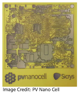
PV Nano Cell, Ltd. (OTC: PVNNF) ("PV Nano Cell" or the "Company"), an innovative provider of inkjet-based conductive digital printing solutions and producer of conductive digital inks, today announced that it has successfully printed and tested high-demanding parts that include printing inside challenging VIA—vertical interconnect access.
VIA are used as an electrical connection between layers (or sides of substrate) in a physical electronic circuit that goes through the plane of one or more adjacent layers. PV Nano Cell was able to print inside VIA with a diameter of 0.6 mm (0.024 inch) and a height of 1 mm (0.04 inch). A phenomenal, minimal resistance of 0.1 ohms was measured and the company said it could print smaller sized VIA as well. One side of the substrate is printed a pattern consisting of multiple widths and thicknesses (heights) of conductive features. This pattern forms an accurate resistor that heats to high temperature in less than milliseconds.
PV Nano Cell’s Chief Executive Officer, Dr. Fernando de la Vega, commented, “In this special application, we first print inside the VIA. Then we print the first designated pattern on one side of the FR-4 (glass-reinforced epoxy laminate material). The substrate is then flipped over and we print the second designated pattern on the other side of the FR-4. The VIA printed in the beginning of the process electrically connects between the two patterns printed on the two sides of the FR-4 substrate. The unique printing process that we developed cuts approximately 50% of the cost of production compared to the existing manufacturing solution. We are positive we can improve the process even more and print smaller-sized VIA.”
PV Nano Cell is implementing these technologies and products to provide a complete solution approach that allows customers to fully realize the potential of inkjet based electronics printing for mass production applications. The company’s proven solution includes its proprietary Sicrys™, silver-based conductive inks, inkjet production printers and the complete printing process.
PV Nano Cell’s Chief of Business Development Officer, Mr. Hanan Markovich commented, "The printed parts have gone through intensive, high-demanding standard testing by the customer and we expect the production to begin in the near future. Such an achievement demonstrates again, the feasibility and attractiveness of PV Nano Cell’s solutions for mass production applications.“
PV Nano Cell, Ltd.
PV Nano Cell (PVN) offers the first-ever complete solution for mass-produced inkjet based, printed electronics. The proven solution includes PVN’s proprietary Sicrys™, silver-based conductive inks, inkjet production printers and the complete printing process. The process includes ink properties' optimization, printer’s parameters setup, printing modifications & tailored printing instructions per application. In the heart of PVN’s value proposition lies its unique and patented conductive silver and coper inks - Sicrys™. Those are the only inks made of Single Nano Crystals – which allows the inks to have the highest stability and throughput required to drive optimal mass-production results for wide range of applications. PVN’s solutions are used all over the world in a range of digital printing applications including: automotive, photovoltaics, printed circuit boards, flexible printed circuits, antennas, sensors, heaters, touchscreens and other. For more information, please visit http://www.pvnanocell.com/
Share on:


Suggested Items
DuPont Unveils Pyralux ML Laminate Series, Offering High Thermal Management for Extreme Environments
04/09/2024 | DuPontDuPont introduced the DuPont™ Pyralux® ML Series of double-sided metal-clad laminates, a unique addition to its extensive family of Pyralux® laminates for flexible and rigid-flex printed circuit boards (PCBs).
Arlon EMD and EMC Announce Expansion in California
03/25/2024 | Arlon EMDArlon EMD, a division of Elite Materials Company (EMC), announces a factory expansion at the Rancho Cucamonga, CA location. Arlon is a global leader in high performance thermoset substrates for mission critical printed circuit boards manufactured for high endurance and long-life programs. Arlon has a 45-year history of manufacturing specialty materials for the Aerospace, Industrial and Military (AIM) markets.
EMC, Arlon Industry Leading PWB Laminates at DesignCon 2024
01/29/2024 | EMCAt the DesignCon 2024 Expo, drop by EMC/ Arlon booth #1260 and learn from the experts with the results from a wide range of performance testing that some of our key OEM customers in almost all market segments of technology, have completed.
Designers Notebook: What Designers Need to Know About Manufacturing, Part 1
01/25/2024 | Vern Solberg -- Column: Designer's NotebookThe designer needs to have a working understanding of two key manufacturing operations: basic circuit board fabrication procedures and assembly process practices. For printed circuit board manufacturing, the number of steps required to produce the printed circuit board correlates to the circuit board's complexity. Greater process complexity in fabricating the circuit board equates to increased costs. To develop any portion of the electronic product, the designer must apply the design for manufacturing (DFM) principles established in the industry. In fact, DFM should always be the goal of the design engineer. It encompasses a wide range of disciplines that must be considered during the planning phase of any product.
Rogers Corporation Exhibiting at DesignCon 2024
01/24/2024 | Rogers CorporationRogers Corporation will exhibit at DesignCon in Santa Clara, CA (booth #609) highlighting some of its high performance circuit materials.