


 It’s Only Common Sense: OCCAM—the Time Is Now
 Marcy's Musings: The Growing Industry
 Dan’s Biz Bookshelf: Seeing the How
Electroplating Through-Holes with Different Geometry: A Novel and High-Productivity Process
June 4, 2015 | Cirexx InternationalEstimated reading time: 1 minute
Microfill through-hole fill (THF) electrolytic copper is a new process designed to offer outstanding through-hole fill, particularly for substrates intended for use as core layers in build–up applications, producing planar, solid copper plugs in high-volume production plating equipment. This technology is intended to replace resin or paste plugging, and offers many advantages, including improved reliability, higher electrical and thermal conductivity, increased productivity and reduced process costs.
This paper describes a novel copper through-hole fill electroplating process designed for use with insoluble anodes and direct current (DC) rectification. The copper through-hole fill chemistry is formulated to operate over a broad range of operating conditions, and offers end-users outstanding production flexibility in either panel or pattern plate operating mode.
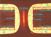
The paper addresses electrolytic copper through-hole filling performance for a variety of substrate thicknesses and hole diameters. The impact of the hole formation method and hole quality on filling ratio and void formation will be discussed. In this work, production scale tests were performed on 100 μm and 200μm thick substrates. The impacts of varying current density and solution flow on hole filling were examined. With optimized deposition conditions, including on-line additive analysis, void-free, highly planar through-hole filling and excellent bottom-up blind microvia filling with low surface copper deposition thickness were demonstrated.
Portability of consumer electronics has become the primary driver for the ever-increasing circuit density of today’s printed circuit designs. Based on the small dimensions of these devices, through-hole and blind via diameters are typically in the 75–150 µm range. Performance improvement and process cost reduction make through-hole filling technology with copper an excellent approach, rather than the conventional plated through-hole.
Prior to the development of electrolytic copper through-hole filling, substrates for such applications were electroplated with a conventional through-hole process, then plugged with an epoxy material. Following these steps, additional planarization, re-metallization and electrolytic copper capping processes were required before the build-up process steps could begin.
Use of electrolytic copper through-hole filling eliminates several of these manufacturing steps and offers a number of additional advantages over the conventional build-up process by enhancing the thermal and electrical conductivity of the interconnections, and by reducing overall costs.
Editor's Note: This article originally appeared in the May 2015 issue of The PCB Magazine.
Share on:


Suggested Items
Designer’s Notebook: What Designers Need to Know About Manufacturing, Part 2
04/24/2024 | Vern Solberg -- Column: Designer's NotebookThe printed circuit board (PCB) is the primary base element for providing the interconnect platform for mounting and electrically joining electronic components. When assessing PCB design complexity, first consider the component area and board area ratio. If the surface area for the component interface is restricted, it may justify adopting multilayer or multilayer sequential buildup (SBU) PCB fabrication to enable a more efficient sub-surface circuit interconnect.
Insulectro’s 'Storekeepers' Extend Their Welcome to Technology Village at IPC APEX EXPO
04/03/2024 | InsulectroInsulectro, the largest distributor of materials for use in the manufacture of PCBs and printed electronics, welcomes attendees to its TECHNOLOGY VILLAGE during this year’s IPC APEX EXPO at the Anaheim Convention Center, April 9-11, 2024.
ENNOVI Introduces a New Flexible Circuit Production Process for Low Voltage Connectivity in EV Battery Cell Contacting Systems
04/03/2024 | PRNewswireENNOVI, a mobility electrification solutions partner, introduces a more advanced and sustainable way of producing flexible circuits for low voltage signals in electric vehicle (EV) battery cell contacting systems.
Heavy Copper PCBs: Bridging the Gap Between Design and Fabrication, Part 1
04/01/2024 | Yash Sutariya, Saturn Electronics ServicesThey call me Sparky. This is due to my talent for getting shocked by a variety of voltages and because I cannot seem to keep my hands out of power control cabinets. While I do not have the time to throw the knife switch to the off position, that doesn’t stop me from sticking screwdrivers into the fuse boxes. In all honesty, I’m lucky to be alive. Fortunately, I also have a talent for building high-voltage heavy copper circuit boards. Since this is where I spend most of my time, I can guide you through some potential design for manufacturability (DFM) hazards you may encounter with heavy copper design.
Trouble in Your Tank: Supporting IC Substrates and Advanced Packaging, Part 5
03/19/2024 | Michael Carano -- Column: Trouble in Your TankDirect metallization systems based on conductive graphite or carbon dispersion are quickly gaining acceptance worldwide. Indeed, the environmental and productivity gains one can achieve with these processes are outstanding. In today’s highly competitive and litigious environment, direct metallization reduces costs associated with compliance, waste treatment, and legal issues related to chemical exposure. What makes these processes leaders in the direct metallization space?