


 The Chemical Connection: Reducing Etch System Water Usage, Part 2
 It’s Only Common Sense: Nice Guys Really Can Finish First
 The Right Approach: I Hear the Train A Comin'
Teltonika Builds First New PCB Plant in Europe in 2 Decades
November 14, 2023 | TeltonikaEstimated reading time: 5 minutes
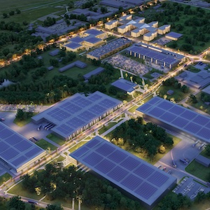
Teltonika, a Lithuanian high-tech company group, is implementing its latest groundbreaking investment project - the construction of a state-of-the-art printed circuit board (PCB) factory in Vilnius, Lithuania. This is one of the ten projects to be established in the Teltonika High-Tech Hill technology park.
This ambitious PCB project is a much-needed link in Teltonika's supply chain, making it a one-stop-shop manufacturer of electronics for product owners across Europe. The PCB factory will emerge in a new Teltonika High-Tech Hill technology park in a 50-ha territory in Vilnius. The high-tech park will house more than ten new facilities, and the investments amount to more than €3.7 billion. It is planned to employ around 6,000 people.
The founder and president of Teltonika IoT Group, Mr Arvydas Paukštys, stated, "We have long excelled in the production of Internet of Things (IoT) products. As we already produce electronics and plastics, now, with the establishment of our PCB factory in Vilnius, we are strategically positioning ourselves to complete our supply chain. This forward-thinking move underscores our commitment to delivering complete high-quality solutions to our customers and solidifies our status as an exceptional partner with a great location for European product owners."
The new PCB factory will be a first-of-its-kind greenfield investment for the PCB industry in Europe in more than two decades. The factory will leverage cutting-edge automation technologies to achieve the highest level of efficiency and precision in PCB production.
Spanning an expansive area of more than 33,000 square meters, the PCB factory will encompass advanced manufacturing facilities and well-appointed administrative premises, ensuring a seamless and efficient production process from start to finish. Teltonika intends to employ around 250 highly qualified specialists at the site.
This ambitious undertaking comes with an estimated budget of €143 million, with a significant portion of the investment earmarked for specialised manufacturing equipment. This substantial financial commitment underscores Teltonika's dedication to delivering the highest quality PCB products and cementing its role as a pioneering industry leader.
Production processes will be fully digitalised to ensure short lead times and optimum production costs. The plant will specialise in the production of PCBs for high-tech products. It will develop technologies for HDI, SBU, and Flex-Rigid, as well as for the design of high-frequency PCBs.
Some of the mass production technology solutions will be used for the first time in Europe. For example, it will be the first plant on the continent to use only digital solder mask printing technology and Vertical Continuous Plating (VCP) for mass production. There will also be a strong focus on ecology, with wastewater and process water from production being treated and recycled back into production, thus minimising and treating the wastewater generated.
Teltonika is supported in this ambitious project by Rico Schluter, who has extensive experience in this market. He has been working in the PCB industry for more than 4 decades and has helped customers build several such plants during his career.
“After working 41 years in the PCB-industry, personally, I am very proud to be a part of this unique project that will give a significant boost to the European PCB industry and its supply chain. Cooperation with Teltonika project team is an absolute pleasure and I am very happy that I can share my very long experience in the PCB industry with my Lithuanian project - team members," says R. Schluter.
The construction of the PCB factory in Vilnius not only marks a significant milestone for Teltonika IoT Group but also reflects a remarkable step forward in the European electronics manufacturing landscape and it’s supply chain. This strategic investment ensures Teltonika's position as a key player in the industry and reinforces Lithuania's status as an emerging hub for advanced electronics manufacturing.
Teltonika IoT Group is poised to continue its excellence in the electronics industry, and the construction of the PCB factory represents a significant leap towards achieving its vision of becoming a one-stop-shop manufacturer for electronics across Europe.
Tomas Auruškevičius, the head of the Teltonika PCB factory, provides more details about the project, which is the first in the Teltonika High-Tech Hill technology park pipeline.
- Tomas, what were the reasons for Teltonika's decision to build a PCB factory?
- The plant is being built for the needs of the Teltonika company group. Due to the low geographical concentration of PCB plants in the region and the steadily growing demand for electronic devices, the investment in the construction of the plant is crucial for the company group's further development. It will also enable us to reduce lead times, minimise supply chain risks, and become independent from third-party political decisions.
The new PCB factory is also dedicated to our existing external customers for whom we provide electronics manufacturing services.
- What factors will make Teltonika's PCB factory unique in Europe?
- First of all, it will be the first greenfield investment for a PCB plant in more than 20 years in Europe.
Secondly, Teltonika’s PCB factory is expected to become one of the most advanced of its kind in Europe. It will ensure the highest possible level of automation and meet the strictest environmental standards. Soldermask InkJet printing for mass production will be implemented first in Europe. Vertical Continuous Plating will be implemented for panel and pattern plating in mass production.
- To date, neither Teltonika nor Lithuania has produced PCBs. What is helping you to master this technology?
- The Teltonika company group has been working in the electronics industry for more than 25 years, so we are experienced specialists in this field. However, when embarking on a project as ambitious as this, we needed the best PCB experts. That is why we are teaming up with Mr Rico Schluter, a very experienced consultant from the PCB industry, working more than 40 years in this industry as CTO and CEO of different companies.
- The Teltonika PCB plant is planned to be operational in early 2025. What will be the production volumes at the start?
- From the beginning, we will start with a production of around 600 m2 of PCB working panels per day in the first phase. Ramping up in few years to 300,000 m2 per year if we are working 24/5. With 24/7 production it will be even more. Therefore, the production volumes depend on a work schedule.
- Can you already disclose which manufacturers' equipment will be installed in Teltonika's PCB factory?
- The contracts with very renowned equipment suppliers from Europe and Asia are recently signed. Our prospective partners include companies such as WISE, Lauffer, Schmoll, Süss MicroTec, Printprocess, ATG, CIMS, KSDW, Elinta Robotic, Adeon, ASS Luippold, Benmayor, Sigma-Mecer and others.
Share on:


Suggested Items
HQ NextPCB of HQ Electronics Debut on the International Stage for Electronics Manufacture at IPC APEX 2024
05/01/2024 | PRNewswireHQ NextPCB of HQ Electronics, a leading Chinese-based multilayer PCB manufacturer and assembly house showcased its industrial prowess on the international stage for the first time at the IPC APEX Expo 2024.
IPC's Vision for Empowering PCB Design Engineers
04/30/2024 | Robert Erickson, IPCAs architects of innovation, printed circuit board designers are tasked with translating increasingly complex concepts into tangible designs that power our modern world. IPC provides the necessary community, standards framework, and education to prepare these pioneers as they explore the boundaries of what’s possible, equipping engineers with the knowledge, skills, and resources required to thrive in an increasingly dynamic field.
On the Line With… Talks With Cadence Expert on SI/PI for PCB Designers
05/02/2024 | I-Connect007In “PCB 3.0: A New Design Methodology—SI/PI for PCB Designers,” subject matter expert Brad Griffin, Cadence Design Systems, discusses how an intelligent system design methodology can move some signal and power integrity decision-making into the physical design space, offering real-time feedback.
USPAE to Springboard U.S. Technology Forward
04/30/2024 | Marcy LaRont, PCB007 MagazineThe U.S. Partnership for Assured Electronics (USPAE) was launched as a nonprofit subsidiary of IPC in 2020, specifically to manage the DoD relationship and access to funding, and to develop a cooperative facility to develop UHDI capabilities in the U.S., not only for the defense sector, but for the whole of the U.S. electronics industry. It is a tall order, but industry veteran Joe O'Neil believes it will happen. Having been tasked with making the UHDI Capable Cooperative Production Facility (UCCPF) a reality, he provides an update on this important project for U.S. electronics manufacturing.
North American PCB Industry Sales Down 23.8% in March
04/29/2024 | IPCIPC announced the March 2024 findings from its North American Printed Circuit Board (PCB) Statistical Program. The book-to-bill ratio stands at 1.13.