


 Punching Out: Breaking Out of the Valuation Box
 Happy’s Tech Talk #28: The Power Mesh Architecture for PCBs
 It’s Only Common Sense: Would You Join Your Own Company?
PE on 3D objects
May 19, 2016 | Barry Matties, I-Connect007Estimated reading time: 13 minutes
I recently sat down with Mike O’Reilly of Optomec to discuss 3D printing onto existing substrates and small polymer-based additive manufacturing pieces and how that impacts PCB manufacturing. Mike also discuss the benefits of printing with conductive epoxies versus the traditional solder process, and where Optomec fits in to the burgeoning 3D market, going forward.
Barry Matties: Mike, why don’t you begin by telling me about your company.
Mike O’Reilly: Optomec’s history is about 25 years old, starting out as a consulting company but reforming as a product company around 1997. We have two divisions now and both are additive manufacturing. One focuses more on the macro scale, for instance, the repair of high-value metal parts for adding material back onto worn parts through the use of our LENS product which fuses powdered metals into fully dense three-dimensional structures, whether it is used to build 3D devices or clad metal onto worn parts.
Then we have the other part of our business, Aerosol Jet, on the micron scale level which really plays primarily into the printed electronics industry—although we are starting to branch into other industries, like medical, etc., where there is an opportunity for next-generation devices that aren't specifically around electronics. They are more about printing micron scale features—10, 20, 30 microns—and developing devices with micro-fluidic channels, etc. We are seeing some very interesting technology and some ramp-up there.
Matties: Where would you say Optomec’s advantage lies in this market?
O’Reilly: In the current marketplace, there really are three or four advantages that Optomec has. The first and foremost advantage is our ability to print onto three-dimensional objects. Our real focus has been printing features, such as a smartphone antenna onto 3D substrates. Typically we are printing antennas directly onto the smartphone injection-molded case in five axes of coordinated motion: on the front, the sides, the back, and filling vias (through-holes) for front-to-back connections. We do this in production, 24 hours a day, 7 days a week, with multiple systems printing thousands of antennas on a weekly basis for commercial use.
Our ability to print onto these devices is made possible by Aerosol Jet’s ability to have a high standoff distance, from one to five millimeters, between the print head nozzle and the surface of the substrate , which allows our solution to print onto complex conformal substrates.
The other advantage we have is a wide operating envelope when it comes to materials. We can print everything from what I like to describe as water to honey. We have different types of atomizers, ultrasonic and pneumatic, that generate small droplets from one to five microns on average that are entrained into an aerosol stream. Viscosities from one to 1,000 centipoise can be atomized. Our unique ability to handle a wide variety of materials has enabled us to service a wide variety of markets, another key product advantage. Lastly, we have unique scaling capability. When I say "unique," I mean that we are a single-nozzle solution—one print head and one atomizer tied together. They can be closely or loosely coupled with each other, but we can multiplex atomizers and print heads together to achieve production throughput.
Let's use an example of laser-direct structuring versus printing antennas. Laser-direct structuring (LDS) is used today to manufacture smartphone antennas. The LDS process requires a specialized polymer used in the injection molding process. LDS then employs a laser to ablate the antenna pattern on the injection molded part. The next step includes electroplating where plating material adheres to the ablated pattern on the injection molded part. Typically, 8–10 microns of copper is plated and then the copper is over-plated with 2–3 microns of nickel. So there are several steps along the way.
Aerosol Jet can be printed on polycarbonate substrates instead of specialized polymers, saving vendors a few cents per device. Think about that cost savings times the number of manufactured smartphones annually. We only need to print 4−6 microns of material, antenna dependent, to get the same frequency performance that is currently realized with the LDS process. The point is that our printing process deposits a lot less material. We only deposit it where you want it to be. Our process doesn’t need a separate bath for plating or two separate baths for two different types of plating material. Our process is much greener than LDS’. After printing antennas onto injection molded parts, an oven sintering process takes place and we are off to the races. Our customers are telling us that our Aerosol Jet printers can help them save significant dollars in their production process. It allows Aerosol Jet customers, such as EMS companies, to bid more competitively offering differentiated production capabilities versus traditional methodologies.
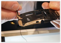
Matties: A piece like this antenna that we are looking at on the case, how long does it take for that?
O’Reilly: This piece would probably take about 60 seconds to print.
Matties: That is pretty quick.
O’Reilly: Remember, we are printing times four in each system. We have four print heads in each system. We have multiple systems. Using this antenna as an example, coupled with a four head system, it then takes about 15 seconds on average per piece.
Matties: When you are talking production volumes, you’ve got to have a stack of machines here.
O’Reilly: For this specific customer production that we have today we have many systems running in parallel with each other—many print heads running 24 hours a day.
Matties: Can the print heads print separate components?
O’Reilly: No, they are all printing the same thing. It's production. Just one after the other. You could certainly go to another machine and say, "Okay. I want a different part." They are all printing the same thing simultaneously.
Aerosol Jet is evolutionary, not revolutionary. If you use LDS today, it is probably already paid for. You already have the infrastructure in place. We are not saying replace that. That would be crazy for us to even think a manufacturer would do that.
However, when the customer runs into a challenge like a next-generation device that may have a metal ring around it, they can't use electroplating. They need to find an alternative to create required device antennas or sensors or whatever functionality they require. If they can't do it with the current manufacturing methodology, our technology may fill this manufacturing gap.
Let me give you another example. Think about printed circuit boards. One of the big challenges, as components get smaller is that traditional dispense systems’ smallest printed feature size (drop) is 120–130 microns which is really pushing the envelope. Most dispense solutions print around 200-micron size features. If we have a 0402 resistor case that is 400 microns long and 200 microns wide and we put down two 200-micron dots, then use the pick and place system on top of the dispensed dots, we are more than likely going to create a short underneath that device. What if we could put down a 50-micron dot? What if it is not solder but a conductive epoxy? That provides customers with the elasticity that they are looking for because with more and more of these smaller mobile devices, there is a lot of ruggedness that has to be built in and the problem with solder is it tends to be rigid and may break if the device is dropped.
We are seeing a big push to print conductive epoxies which provide customers with the performance and flexibility they are looking for. The need for printed epoxies started in the mil-aero sector and now is making its way into consumer-oriented manufacturing companies.
We say use your existing equipment because 90% of what you are doing is traditional, but when your manufacturing equipment is not capable of meeting your needs our systems can fill the manufacturing gap and become just another step in a customer’s manufacturing process. That is how we see ourselves as evolutionary and not revolutionary.
We believe that manufacturing companies have proven processes in place and to disrupt those processes is extremely difficult and extremely disconcerting for them. Why not just add something in their process that is not disruptive and can service their needs? Eventually, once customers see value in our technology, we can expand out from there.
Matties: It seems like they will. It seems like all of this is in its infancy, really.
O’Reilly: It is. We have been in the business as an additive manufacturing company for 12–15 years. We introduced our product in 2004 and shipped our very first system developed by PhDs, very interesting technology. We have sold over 150 of these systems over the past 12 years. It was about two years ago, when we really started to take off as manufacturing companies were looking for product to fill their production gaps.
We matured as a company. We built more repeatable and reliable equipment. We brought in production oriented engineers that really understood how to build equipment and we are running, as I said, 24/7 in EMS companies, who are very conservative folks. In production they are achieving 95% yields. Yeah, they would like to be 98%. Today, we're 95% and I think for a second-generation product that’s pretty good.
Page 1 of 2
Share on:


Suggested Items
Connect the Dots: Designing for Reality—The Pre-Manufacturing Process
05/08/2024 | Matt Stevenson -- Column: Connect the DotsI have been working with Nolan Johnson on a podcast series about designing PCBs for the reality of manufacturing. By sharing lessons learned over a long career in the PCB industry, we hope to shorten learning curves and help designers produce better boards with less hassle and rework. Episode 2 deals with the electronic pre-manufacturing process. Moving from CAD (computer-aided design) to CAM (computer-aided manufacturing) is a key step in PCB manufacturing. CAM turns digital designs into instructions that machines can use to actually build the PCB.
AIM Solder Signs Shinil Fl Ltd. as New Distributor for Korea
05/08/2024 | AIM SolderAIM Solder, a leading global manufacturer of solder assembly materials for the electronics industry, is pleased to announce a new distribution partnership with Shinil Fl Ltd., a prominent supplier of technological solutions in the SMT and semiconductor sectors.
Indium Corporation to Showcase HIA Materials at ECTC
05/07/2024 | Indium CorporationAs an industry leader in innovative materials solutions for semiconductor packaging and assembly, Indium Corporation® will feature its advanced products designed to meet the evolving challenges of heterogeneous integration and assembly (HIA) and fine-pitch system-in-package (SiP) applications at the 74th Electronic Components and Technology Conference (ECTC), May 28‒31, in Denver, Colorado.
Indium Corporation Expert to Present on Pb-Free Solder for Die-Attach in Discrete Power Applications
04/30/2024 | Indium CorporationIndium Corporation Product Manager – Semiconductor Dean Payne will present at the Advanced Packaging for Power Electronics conference, hosted by IMAPS, held May 8-9 in Woburn, Massachusetts, USA.
Taiyo Circuit Automation Installs New DP3500 into Fuba Printed Circuits, Tunisia
04/25/2024 | Taiyo Circuit AutomationTaiyo Circuit Automation is proud to be partnered with Fuba Printed Circuits, Tunisia part of the OneTech Group of companies, a leading printed circuit board manufacturer based out of Bizerte, Tunisia, on their first installation of Taiyo Circuit Automation DP3500 coater.