-

- News
- Books
Featured Books
- pcb007 Magazine
Latest Issues
Current Issue
The Growing Industry
In this issue of PCB007 Magazine, we talk with leading economic experts, advocacy specialists in Washington, D.C., and PCB company leadership to get a well-rounded picture of what’s happening in the industry today. Don’t miss it.

The Sustainability Issue
Sustainability is one of the most widely used terms in business today, especially for electronics and manufacturing but what does it mean to you? We explore the environmental, business, and economic impacts.
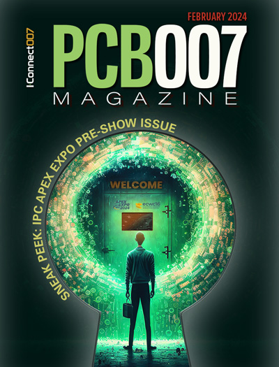
The Fabricator’s Guide to IPC APEX EXPO
This issue previews many of the important events taking place at this year's show and highlights some changes and opportunities. So, buckle up. We are counting down to IPC APEX EXPO 2024.
- Articles
Article Highlights
- Columns
Search Console
- Links
- Events
||| MENU - pcb007 Magazine
14th Electronic Circuits World Convention
June 20, 2017 | Happy HoldenEstimated reading time: 10 minutes
The 14th Electronic Circuits World Convention (ECWC14) got started in Seoul to the usual fanfare after the opening ceremonies of the KPCA 2017 Show. The ribbon-cutting ceremony was conducted by KPCA’s Jung Bong Hong and the representatives of the other WECC members: WECC Secretary General Rex Rozario; Jin Zhangi (CPCA); Alun Morgan (EIPC); Vikram Desai (Electronic Industries Association of India); Canice Chung (Hong Kong PCA); David Bergman (IPC); Kushal Patel (IPCA); Toshifumi Kobayashi (JPCA), and Rich Wu (TPCA). The event took place in the KINTEX Gyeonggi-do Exhibition Center, a large venue with a mall on the first floor (Figure 1).
Figure 1: The ribbon-cutting ceremony opening ECWC14 in Seoul, Korea.
Award-Winning Papers
Six papers were selected by the ECWC14 Technical Committee. The six winners were rewarded with prizes (Figure 2). These papers are highlighted in the Program with an “AP.” One paper was “Sharing Experience in Embedding of Active and Passive Components in Organic PCBs for More Reliability and Miniaturization,” by Thomas Hofmann, of Hofmann Leiterplatten GMBH. The paper was just published in the June 2017 issue of The PCB Magazine.
Other Notable Papers
Twenty-one papers were cancelled at the last moment because the authors from China could not get exit visas and were unable to attend the conference to deliver their papers. These papers were converted to posters (a total of 23) and a summary was available to attendees. The papers were included in the proceedings.
Figure 2: The six authors receive their “Best Paper” awards at the welcoming reception at ECWC14. (Courtesy of KPCA)
“Packaging Technology in 2017 and Beyond,” Young Chul Park, Amkor Technology Korea.
The first keynote was from the president of Amkor Technology Korea, who highlighted the main areas of top technology trends: Industry 4.0; artificial intelligence (AI); Internet of Things (IoT); data centers; and 5G telecommunications. Industry has five big things to meet requirements for these trends:
- Mobility—The industry demand is for smaller form factors with more integration including thinner, flexible and foldable capability, all at a lower cost. Current thickness of LCD displays is 240 µm.
- IoT—The industry demands are for smaller form factor with better performance and better reliability. These devices will be produced in extremely high volumes and will be a major user of the 5G millimeter wave-length (30 to 300 GHz) wireless infrastructure. Advanced design rules will be employed, as well as advanced structures of embedding while using low-loss materials with superior high-speed foils and treatments.
- Automotive—The industry demand is for zero defects and perfect reliability! The life of an auto is at least 15 years or more, so these assemblies require much longer operation times require extremely high quality and reliability, even when operating down to -40°C or as high as 155°C in high-humidity environments.
- HPC—The industry demand is for performance 100,000 times greater than the single PC. This generates an enormous need for power and for cooling all the heat generated. The Facebook data center was built on the edge of the Arctic Circle in Lulea, Sweden.
- Memory—The industry demand is for high bandwidth performance in the 480 GB per sec. Range. Various operating condition will require hybrid packaging methodologies with thin PKG heights, at lower cosummation: “Many global electronic equipment volume markets (except automotive, medical & SEMI equipment) have been stagnant; emerging new products are not yet large. 2016 closed optimistically with seasonally strong semiconductor shipments and positive leading indicators. Copper foil shortages are impacting PCB growth.”
These conclusions are illustrated in Figure 3, showing the world’s electronic equipment monthly shipments. Walt documented the “maturing” of the PC platforms but expounded on future volume markets like: smart cars, 5G handsets and infrastructure, the IoT, drones, wearables and automation/robotic applications. These all call for more semiconductors of microprocessors, memory and communications chips. (All amounts are in US dollars.)
Page 1 of 6
Suggested Items
Designer’s Notebook: What Designers Need to Know About Manufacturing, Part 2
04/24/2024 | Vern Solberg -- Column: Designer's NotebookThe printed circuit board (PCB) is the primary base element for providing the interconnect platform for mounting and electrically joining electronic components. When assessing PCB design complexity, first consider the component area and board area ratio. If the surface area for the component interface is restricted, it may justify adopting multilayer or multilayer sequential buildup (SBU) PCB fabrication to enable a more efficient sub-surface circuit interconnect.
Insulectro’s 'Storekeepers' Extend Their Welcome to Technology Village at IPC APEX EXPO
04/03/2024 | InsulectroInsulectro, the largest distributor of materials for use in the manufacture of PCBs and printed electronics, welcomes attendees to its TECHNOLOGY VILLAGE during this year’s IPC APEX EXPO at the Anaheim Convention Center, April 9-11, 2024.
ENNOVI Introduces a New Flexible Circuit Production Process for Low Voltage Connectivity in EV Battery Cell Contacting Systems
04/03/2024 | PRNewswireENNOVI, a mobility electrification solutions partner, introduces a more advanced and sustainable way of producing flexible circuits for low voltage signals in electric vehicle (EV) battery cell contacting systems.
Heavy Copper PCBs: Bridging the Gap Between Design and Fabrication, Part 1
04/01/2024 | Yash Sutariya, Saturn Electronics ServicesThey call me Sparky. This is due to my talent for getting shocked by a variety of voltages and because I cannot seem to keep my hands out of power control cabinets. While I do not have the time to throw the knife switch to the off position, that doesn’t stop me from sticking screwdrivers into the fuse boxes. In all honesty, I’m lucky to be alive. Fortunately, I also have a talent for building high-voltage heavy copper circuit boards. Since this is where I spend most of my time, I can guide you through some potential design for manufacturability (DFM) hazards you may encounter with heavy copper design.
Trouble in Your Tank: Supporting IC Substrates and Advanced Packaging, Part 5
03/19/2024 | Michael Carano -- Column: Trouble in Your TankDirect metallization systems based on conductive graphite or carbon dispersion are quickly gaining acceptance worldwide. Indeed, the environmental and productivity gains one can achieve with these processes are outstanding. In today’s highly competitive and litigious environment, direct metallization reduces costs associated with compliance, waste treatment, and legal issues related to chemical exposure. What makes these processes leaders in the direct metallization space?
