


 The Right Approach: I Hear the Train A Comin'
 It’s Only Common Sense: OCCAM—the Time Is Now
 Marcy's Musings: The Growing Industry
Zuken Showcases DFM Solutions at PCB West 2017
September 6, 2017 | ZukenEstimated reading time: 2 minutes
Zuken USA is again participating in PCB West, to be held September 12-14 in Santa Clara, California. The event includes a three-day technical conference and one-day exhibition to be held at the Santa Clara Convention Center.
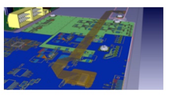
Zuken and Nano Dimension will share a booth and showcase the latest technologies for DFM and 3D printing. Zuken’s CR-8000 Design Force DfM software provides a platform to automate the process of applying the necessary rules for different board technologies, including flex, with the benefit of improving design quality and manufacturing yields. This software incorporates a database of design rules for many different manufacturing processes that take into account materials and technologies.
Nano Dimension will feature its DragonFly 2020 3D printer for professional electronics and nanotechnology-based conductive and dielectric materials for its 3D printers. DragonFly 2020 3D Printers enable companies involved in electronics to take control of their development cycles by 3D printing their own multi-layer PCB prototypes. The 3D printer continues to capture global industry and media attention.
Together, the companies’ combined offerings represent a complete solution for the design and manufacture of multi-layer PCBs unmatched in the industry. By using them together, development teams can introduce more agile development processes at every prototyping stage – from concept verification and design validation, to test fixtures. With these solutions, users can expect to spend more time innovating and getting new ideas to market, rather than dealing with design administration.
The two companies are presenting multiple sessions during the technical conference highlighting their technology expertise:
- Power Integrity and Decoupling Primer for PCB Designers
- Improve Flexible Printed Circuit Manufacturing Productivity with Better DfM Checks
- EDA Support and Roadmap for 3D Printing of PCBs
- 3D Printing: A New Dimension in Electronics Prototyping & Manufacturing
About Zuken
Zuken is a global provider of leading-edge software and consulting services for electrical and electronic design and manufacturing. Founded in 1976, Zuken has the longest track record of technological innovation and financial stability in the electronic design automation (EDA) software industry. The company’s extensive experience, technological expertise and agility, combine to create world-class software solutions. Zuken’s transparent working practices and integrity in all aspects of business produce long-lasting and successful customer partnerships that make Zuken a reliable long-term business partner.
Zuken is focused on being a long-term innovation and growth partner. The security of choosing Zuken is further reinforced by the company’s people—the foundation of Zuken’s success. Coming from a wide range of industry sectors, specializing in many different disciplines and advanced technologies, Zuken’s people relate to and understand each company’s unique requirements. For more information about the company and its products, click here.
About Nano Dimension Ltd.
Nano Dimension is a leading additive manufacturing technology company. Nano Dimension is disrupting, reshaping and defining the future of how electronics are made. With its unique 3D printing technologies, Nano Dimension is targeting the growing demand for electronic devices that require increasingly sophisticated features and rely on printed circuit boards (PCBs). Demand for circuitry, including PCBs -which are the heart of every electronic device - covers a diverse range of industries, including consumer electronics, medical devices, defense, aerospace, automotive, IoT and telecom. These sectors can all benefit greatly from Nano Dimension’s 3D printed electronics solutions for rapid prototyping and short-run manufacturing.
Share on:


Suggested Items
Warm Windows and Streamlined Skin Patches – IDTechEx Explores Flexible and Printed Electronics
04/26/2024 | IDTechExFlexible and printed electronics can be integrated into cars and homes to create modern aesthetics that are beneficial and easy to use. From luminous car controls to food labels that communicate the quality of food, the uses of this technology are endless and can upgrade many areas of everyday life.
Book Excerpt: The Printed Circuit Assembler’s Guide to... Factory Analytics
04/24/2024 | I-Connect007 Editorial TeamIn our fast-changing, deeply competitive, and margin-tight industry, factory analytics can be the key to unlocking untapped improvements to guarantee a thriving business. On top of that, electronics manufacturers are facing a tremendous burden to do more with less. If you don't already have a copy of this book, what follows is an excerpt from the introduction chapter of 'The Printed Circuit Assembler’s Guide to... Factory Analytics: Unlocking Efficiency Through Data Insights' to whet your appetite.
Listen Up! The Intricacies of PCB Drilling Detailed in New Podcast Episode
04/25/2024 | I-Connect007In episode 5 of the podcast series, On the Line With: Designing for Reality, Nolan Johnson and Matt Stevenson continue down the manufacturing process, this time focusing on the post-lamination drilling process for PCBs. Matt and Nolan delve into the intricacies of the PCB drilling process, highlighting the importance of hole quality, drill parameters, and design optimization to ensure smooth manufacturing. The conversation covers topics such as drill bit sizes, aspect ratios, vias, challenges in drilling, and ways to enhance efficiency in the drilling department.
Elevating PCB Design Engineering With IPC Programs
04/24/2024 | Cory Blaylock, IPCIn a monumental stride for the electronics manufacturing industry, IPC has successfully championed the recognition of the PCB Design Engineer as an official occupation by the U.S. Department of Labor (DOL). This pivotal achievement not only underscores the critical role of PCB design engineers within the technology landscape, but also marks the beginning of a transformative journey toward nurturing a robust, skilled workforce ready to propel our industry into the future.
Winner of The Science Show Rakett 69 Receives Incap Scholarship
04/24/2024 | IncapThe winner of the Rakett 69 science show, Andri Türkson, who stood out as an electronics enthusiast, received a scholarship from Incap Estonia, along with an internship opportunity in Saaremaa.