-

- News
- Books
Featured Books
- pcb007 Magazine
Latest Issues
Current Issue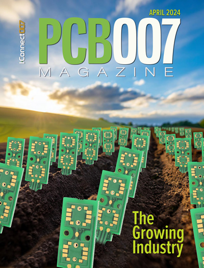
The Growing Industry
In this issue of PCB007 Magazine, we talk with leading economic experts, advocacy specialists in Washington, D.C., and PCB company leadership to get a well-rounded picture of what’s happening in the industry today. Don’t miss it.

The Sustainability Issue
Sustainability is one of the most widely used terms in business today, especially for electronics and manufacturing but what does it mean to you? We explore the environmental, business, and economic impacts.

The Fabricator’s Guide to IPC APEX EXPO
This issue previews many of the important events taking place at this year's show and highlights some changes and opportunities. So, buckle up. We are counting down to IPC APEX EXPO 2024.
- Articles
Article Highlights
- Columns
Search Console
- Links
- Events
||| MENU - pcb007 Magazine
The PCB Norsemen: The Velocity of Technology— What Does It Really Mean?
July 2, 2018 | Jan Pedersen, ELMATICAEstimated reading time: 2 minutes
Speed and Direction— Where Are we Going?
The subtitle of IPC APEX EXPO 2018 was “Succeed at The Velocity of Technology.” What did IPC mean by this?
I have not asked the IPC staff what this phrase meant in real terms, but I have my own interpretation. For me, the velocity of technology has two components: speed and direction. The technology in electronics develops faster than ever. A user of mobile phones or computers may not understand the rate at which electronics changes, but if you see the development of components and the complexity of today’s packages, you understand the speed.
Driving a car is probably one of the areas where the user comes in direct touch with the technology development. And we understand the speed when we see how fast we get new versions of smartphones and other gadgets. But in what direction are we going? We all know that size and weight reduction is good. We get more function into the same space. At the same time, we increase the functionality— a mobile phone today can do more than a desktop computer did some years ago. It has a better camera than the reasonably good full-size digital camera we still have in our drawers.
I am a PCB geek. For me, it is interesting to see how technology development has affected the PCB, and in which direction we move. How do we see the velocity of technology in PCBs?
(Almost) Born and Raised in a PCB Plant
I was born in a PCB plant outside Oslo in June 1958. Norway had no PCB factories at that time, so my father saw the potential and started to etch boards in a garage using silkscreened etching resist and ferric chloride etchant. The boards had to be used fast to avoid corrosion; we only had a simple lacquer to protect the copper.
Time went by and at 20-something I was set to lead a small PTH plant. We started to use photoimageable plating resist and infrared re flow for tin-lead (those machines typically had a small fire every week). At that time, we had no RoHS, REACH or ISO 14000 or really any environmental awareness. I have some stories that are better told in more private circles.
In 1992, I joined Elmatica and during the ‘90s we saw some development of PCB technology but mostly just a slight miniaturization. Frankly speaking, the PCB technology itself has not changed that much today either. We still print and etch. We still drill, but we use a laser in addition to the mechanical drills. We still print solder mask, we still plate copper to achieve required thickness and through-hole connections. So, we have seen some changes, but not the speed or change of direction as in other technologies.
The velocity of PCB technology today is still, from my point of view, not at the same rate as we see in components. The introduction of smaller components has almost out-challenged the PCB. But only just. And, we are still in the same direction, so we cannot brag too much about the velocity of the PCB technology.
To read the full version of this article which originally appeared in the May 2018 issue of PCB007 Magazine, click here.
Suggested Items
Taiyo Circuit Automation Installs New DP3500 into Fuba Printed Circuits, Tunisia
04/25/2024 | Taiyo Circuit AutomationTaiyo Circuit Automation is proud to be partnered with Fuba Printed Circuits, Tunisia part of the OneTech Group of companies, a leading printed circuit board manufacturer based out of Bizerte, Tunisia, on their first installation of Taiyo Circuit Automation DP3500 coater.
Vicor Power Orders Hentec Industries/RPS Automation Pulsar Solderability Testing System
04/24/2024 | Hentec Industries/RPS AutomationHentec Industries/RPS Automation, a leading manufacturer of selective soldering, lead tinning and solderability test equipment, is pleased to announce that Vicor Power has finalized the purchase of a Pulsar solderability testing system.
AIM Solder’s Dillon Zhu to Present on Ultraminiature Soldering at SMTA China East
04/22/2024 | AIMAIM Solder, a leading global manufacturer of solder assembly materials for the electronics industry, is pleased to announce that Dillon Zhu will present on the topic: Ultraminiature Soldering: Techniques, Technologies, and Standards at SMTA China East. This event is being held at the Shanghai World Expo Exhibition & Convention Center from April 24-25.
AIM to Highlight NC259FPA Ultrafine No Clean Solder Paste at SMTA Wisconsin Expo & Tech Forum
04/18/2024 | AIMAIM Solder, a leading global manufacturer of solder assembly materials for the electronics industry, is pleased to announce its participation in the upcoming SMTA Wisconsin Expo & Tech Forum taking place on May 7 at the Four Points by Sheraton | Milwaukee Airport, in Milwaukee, Wisconsin.
Hentec/RPS Publishes an Essential Guide to Selective Soldering Processing Tech Paper
04/17/2024 | Hentec Industries/RPS AutomationHentec Industries/RPS Automation, a leading manufacturer of selective soldering, lead tinning and solderability test equipment, announces that it has published a technical paper describing the critical process parameters that need to be optimized to ensure optimal results and guarantee the utmost in end-product quality.
