


 The Right Approach: I Hear the Train A Comin'
 It’s Only Common Sense: OCCAM—the Time Is Now
 Marcy's Musings: The Growing Industry
Atotech to Exhibit and Present at the SEMICON Taiwan Show
August 30, 2018 | AtotechEstimated reading time: 2 minutes
Atotech will participate at this year’s SEMICON Taiwan Show, held from September 5 to 7, 2018, in the Taipei Nangang Exhibition Center Hall 1 in Taipei, Taiwan. The Atotech team can be found at booth J2340 and at the SiP Global Summit where Dr. Ralf Schmidt, R&D Manager Semiconductor at Atotech Group, will exemplify the company’s answer for enhanced reliability of sub 5 µm L/S RDL for 5G.
“Next generation devices for FOWLP require the reduction of the RDL pitch to 1x1 µm or less. This leads to an increased importance of the mechanical properties. Recent findings point out the importance of the formation of a proper composite with the subjacent substrate, i.e. polyimide (PI). The composite formation can strongly improve the mechanical properties and, thus, the reliability of the Cu lines,” states Ralf.
In his presentation on Thursday, September 6, 2018, from 3:45 pm to 4:15 pm, Ralf will discuss the different solutions to promote the formation of a proper composite material consisting of Cu RDL lines and PI, especially with respect to their influence on mechanical properties as well as their suitability for potential 5G applications. The combination of high purity Cu deposits and strong composite formations with the substrate is considered to be a key parameter for future sub 5 µm L/S multilayer RDL technologies.
The company also announced a special product feature on Spherolyte UF3, a new wet chemical process solution for next generation RDLs in FOWLP, and MultiPlate, the company's new production tool for the simultaneous copper deposition for embedded power chips, at booth number J2340.
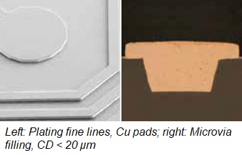
Spherolyte UF3
This product allows for fine line RDL plating and microvia filling in one process. Advantages include the low internal stress of less than 20 MPa and the low incorporation level of additives which enables high purity Cu deposits. Spherolyte UF3 also reduces Cu line breakages after thermal cycle testing.
MultiPlate for Power ICs
MultiPlate for power ICs was developed for the simultaneous copper deposition for embedding power chips and backside metallization. The Atotech tool allows for plating on 150, 200 and 300 mm wafers including Taiko thin wafers and panel sizes of up to 600 x 600 mm. The dual side metallization process minimizes warpage and enables high deposition uniformity at high plating speeds. This leads to a process cost reduction of up to 26 percent, and reduces the number of process steps by 25 percent, as compared to sequential processing.
About Atotech
Atotech is one of the world’s leading manufacturers of specialty chemicals and equipment for the printed circuit board, IC-substrate and semiconductor industries, as well as for the decorative and functional surface finishing industries. Atotech has annual sales of $1.2 billion (2017). The company is fully committed to sustainability – we develop technologies to minimize waste and to reduce environmental impact. Atotech has its headquarters in Berlin, Germany, and employs about 4,000 people in over 40 countries. For more information, click here.
Share on:


Suggested Items
Designer’s Notebook: What Designers Need to Know About Manufacturing, Part 2
04/24/2024 | Vern Solberg -- Column: Designer's NotebookThe printed circuit board (PCB) is the primary base element for providing the interconnect platform for mounting and electrically joining electronic components. When assessing PCB design complexity, first consider the component area and board area ratio. If the surface area for the component interface is restricted, it may justify adopting multilayer or multilayer sequential buildup (SBU) PCB fabrication to enable a more efficient sub-surface circuit interconnect.
Insulectro’s 'Storekeepers' Extend Their Welcome to Technology Village at IPC APEX EXPO
04/03/2024 | InsulectroInsulectro, the largest distributor of materials for use in the manufacture of PCBs and printed electronics, welcomes attendees to its TECHNOLOGY VILLAGE during this year’s IPC APEX EXPO at the Anaheim Convention Center, April 9-11, 2024.
ENNOVI Introduces a New Flexible Circuit Production Process for Low Voltage Connectivity in EV Battery Cell Contacting Systems
04/03/2024 | PRNewswireENNOVI, a mobility electrification solutions partner, introduces a more advanced and sustainable way of producing flexible circuits for low voltage signals in electric vehicle (EV) battery cell contacting systems.
Heavy Copper PCBs: Bridging the Gap Between Design and Fabrication, Part 1
04/01/2024 | Yash Sutariya, Saturn Electronics ServicesThey call me Sparky. This is due to my talent for getting shocked by a variety of voltages and because I cannot seem to keep my hands out of power control cabinets. While I do not have the time to throw the knife switch to the off position, that doesn’t stop me from sticking screwdrivers into the fuse boxes. In all honesty, I’m lucky to be alive. Fortunately, I also have a talent for building high-voltage heavy copper circuit boards. Since this is where I spend most of my time, I can guide you through some potential design for manufacturability (DFM) hazards you may encounter with heavy copper design.
Trouble in Your Tank: Supporting IC Substrates and Advanced Packaging, Part 5
03/19/2024 | Michael Carano -- Column: Trouble in Your TankDirect metallization systems based on conductive graphite or carbon dispersion are quickly gaining acceptance worldwide. Indeed, the environmental and productivity gains one can achieve with these processes are outstanding. In today’s highly competitive and litigious environment, direct metallization reduces costs associated with compliance, waste treatment, and legal issues related to chemical exposure. What makes these processes leaders in the direct metallization space?