


 The Right Approach: I Hear the Train A Comin'
 It’s Only Common Sense: OCCAM—the Time Is Now
 Marcy's Musings: The Growing Industry
Atotech to Present at the Electronics Packaging Technology Conference 2018 in Singapore
November 22, 2018 | AtotechEstimated reading time: 1 minute
Atotech will present at this year’s Electronics Packaging Technology Conference (EPTC) held at the Resorts World Sentosa in Singapore from December 4 to 7, 2018.
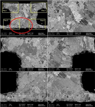
Image Caption: SEM micrographs of copper structure after annealing (125°C, 4h) deposited at 3 ASD with the novel chemistry
On December 6, 2018, from 5:00 to 5:25 pm, in Room Leo 2, Mustafa Oezkoek, Global Product Manager Panel and Pattern Plating at Atotech Group, will present “Enhancing productivity for IC-substrate manufacturing by using a novel copper electrolyte for Semi Additive Plating (SAP).”
In his presentation, Mustafa will introduce a new SAP copper electrolyte which allows for higher current densities while still keeping very good copper thickness within unit distribution (WUD) results.
“When operating with lines and spaces (L/S) of 10/10 μm and less, copper thickness variation is one of the critical parameters, which have to be controlled within a tight range in order to avoid reliability problems in assembly or during the lifetime. Another important parameter is the current density used for the copper plating process. The current density is important for the productivity but also impacts the surface thickness distribution which is not beneficial for the quality of the product,” states Mustafa. “We have developed an electrolyte which overcomes this conflict of productivity and copper thickness variation. Besides several beneficial parameters, its main benefit is its capability to operate at > 3 A/dm², which brings an improvement of the productivity by a factor of almost two.”
Visitors to the EPTC are welcome to join the presentation and discuss this and further market-leading new developments with Mustafa following the presentation.
About Atotech
Atotech is one of the world’s leading manufacturers of specialty chemicals and equipment for the printed circuit board, IC-substrate and semiconductor industries, as well as for the decorative and functional surface finishing industries. Atotech has annual sales of USD1.2 billion (2017). The company is fully committed to sustainability – we develop technologies to minimize waste and to reduce environmental impact. Atotech has its headquarters in Berlin, Germany, and employs about 4,000 people in over 40 countries. For more information, click here.
Share on:


Suggested Items
Designer’s Notebook: What Designers Need to Know About Manufacturing, Part 2
04/24/2024 | Vern Solberg -- Column: Designer's NotebookThe printed circuit board (PCB) is the primary base element for providing the interconnect platform for mounting and electrically joining electronic components. When assessing PCB design complexity, first consider the component area and board area ratio. If the surface area for the component interface is restricted, it may justify adopting multilayer or multilayer sequential buildup (SBU) PCB fabrication to enable a more efficient sub-surface circuit interconnect.
Insulectro’s 'Storekeepers' Extend Their Welcome to Technology Village at IPC APEX EXPO
04/03/2024 | InsulectroInsulectro, the largest distributor of materials for use in the manufacture of PCBs and printed electronics, welcomes attendees to its TECHNOLOGY VILLAGE during this year’s IPC APEX EXPO at the Anaheim Convention Center, April 9-11, 2024.
ENNOVI Introduces a New Flexible Circuit Production Process for Low Voltage Connectivity in EV Battery Cell Contacting Systems
04/03/2024 | PRNewswireENNOVI, a mobility electrification solutions partner, introduces a more advanced and sustainable way of producing flexible circuits for low voltage signals in electric vehicle (EV) battery cell contacting systems.
Heavy Copper PCBs: Bridging the Gap Between Design and Fabrication, Part 1
04/01/2024 | Yash Sutariya, Saturn Electronics ServicesThey call me Sparky. This is due to my talent for getting shocked by a variety of voltages and because I cannot seem to keep my hands out of power control cabinets. While I do not have the time to throw the knife switch to the off position, that doesn’t stop me from sticking screwdrivers into the fuse boxes. In all honesty, I’m lucky to be alive. Fortunately, I also have a talent for building high-voltage heavy copper circuit boards. Since this is where I spend most of my time, I can guide you through some potential design for manufacturability (DFM) hazards you may encounter with heavy copper design.
Trouble in Your Tank: Supporting IC Substrates and Advanced Packaging, Part 5
03/19/2024 | Michael Carano -- Column: Trouble in Your TankDirect metallization systems based on conductive graphite or carbon dispersion are quickly gaining acceptance worldwide. Indeed, the environmental and productivity gains one can achieve with these processes are outstanding. In today’s highly competitive and litigious environment, direct metallization reduces costs associated with compliance, waste treatment, and legal issues related to chemical exposure. What makes these processes leaders in the direct metallization space?