


 It’s Only Common Sense: Nice Guys Really Can Finish First
 The Right Approach: I Hear the Train A Comin'
 Marcy's Musings: The Growing Industry
Atotech to Present at IPC APEX EXPO 2019
January 23, 2019 | AtotechEstimated reading time: 2 minutes
Atotech to present a new high-throw electroless Cu bath, through-hole, BMV filling, and conformal plating electrolyte, and its revolutionary direct pure EPAG final finish at the IPC APEX EXPO 2019.
BERLIN, January 23, 2019: Atotech is one of the world’s leading suppliers of specialty chemicals and equipment for the printed circuit board, package substrate and semiconductor industry. At one of the industry’s premier events, the IPC APEX Expo held at the San Diego Convention Center in San Diego, USA, from January 26 to 31, 2019, the company will exhibit and present on several new product developments.
On Tuesday, January 29, from 1:30 to 3:00 p.m., Moody Dreiza, Business Director for Electronics, North America, at Atotech USA LLC, will present “Copper Filling of Blind Microvias, Through-Holes and Cu Pillar Plating - The Present and the Future” in session S02 “PCB fabrication / Plating I”. “I will describe the reasons for development and a roadmap of dimensions for copper filled through-holes, blind microvias and other copper plated structures on PCBs by presenting aspect ratios, dimensions and results of plated through-holes used today in high volume manufacturing for blind microvia and through-hole filling with electroplated copper,” states Moody. His presentation will include feasibility studies of new electroplated structures for future applications such as copper pillar plating on IC-substrates.
On Wednesday, January 30, from 10:30 a.m. to 12:00 p.m., Roger Massey, Technical Marketing Manager at Atotech Group, will present “Developments in Electroless Copper Processes to Improve Performance in amSAP Mobile Applications” in session S13 “PCB Fabrication and Plating II”. In his presentation, Roger will highlight the benefits and robust performance of a newly developed electroless copper process for amSAP applications.
On Wednesday, January 30, from 3:30 to 4:30 p.m., Sandra Nelle, Product Manager for Surface Finishing at Atotech Group, will present “Designing a High Performance Electroless Nickel and Immersion Gold to Maximize Highest Reliability” in session S23 “PCB Surface Finishes II”. Sandra will elaborate on whether there are any ‘value added’ benefits to an HP ENIG. “I will also use data generated by Design of Experiment (DOE) to elaborate the impact of electroless nickel variables in combination with traditional and cyanide-free immersion gold on recognized quality expectations,” adds Sandra.
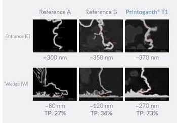
Printoganth T1 – Throwing Power Comparison
Atotech experts will also be on hand to discuss the latest chemistry and equipment at booth 311. Atotech’s latest products will be showcased at the booth, including:
- Printoganth T1, a brand new high-throw electroless copper process for advanced HDI and amSAP technology
- Inpulse 2THF, a versatile electrolyte for through-hole, blind microvia, and conformal plating for advanced HDI and substrate technology
- PallaBond, a revolutionary direct pure EPAG final finish for real fine / line applications
- Uniplate PLB Cu, a high throughput horizontal systems solution for desmear and metallization, that offers best cost, performance, and quality results in combination with Atotech’s Printoganth® T1 and Inpulse 2THF process chemistry
About Atotech
Atotech is one of the world’s leading manufacturers of specialty chemicals and equipment for the printed circuit board, IC-substrate and semiconductor industries, as well as for the decorative and functional surface finishing industries. Atotech has annual sales of $1.2 billion (2017). The company is fully committed to sustainability – we develop technologies to minimize waste and to reduce environmental impact. Atotech has its headquarters in Berlin, Germany, and employs about 4,000 people in over 40 countries.
Share on:


Suggested Items
Designer’s Notebook: What Designers Need to Know About Manufacturing, Part 2
04/24/2024 | Vern Solberg -- Column: Designer's NotebookThe printed circuit board (PCB) is the primary base element for providing the interconnect platform for mounting and electrically joining electronic components. When assessing PCB design complexity, first consider the component area and board area ratio. If the surface area for the component interface is restricted, it may justify adopting multilayer or multilayer sequential buildup (SBU) PCB fabrication to enable a more efficient sub-surface circuit interconnect.
Insulectro’s 'Storekeepers' Extend Their Welcome to Technology Village at IPC APEX EXPO
04/03/2024 | InsulectroInsulectro, the largest distributor of materials for use in the manufacture of PCBs and printed electronics, welcomes attendees to its TECHNOLOGY VILLAGE during this year’s IPC APEX EXPO at the Anaheim Convention Center, April 9-11, 2024.
ENNOVI Introduces a New Flexible Circuit Production Process for Low Voltage Connectivity in EV Battery Cell Contacting Systems
04/03/2024 | PRNewswireENNOVI, a mobility electrification solutions partner, introduces a more advanced and sustainable way of producing flexible circuits for low voltage signals in electric vehicle (EV) battery cell contacting systems.
Heavy Copper PCBs: Bridging the Gap Between Design and Fabrication, Part 1
04/01/2024 | Yash Sutariya, Saturn Electronics ServicesThey call me Sparky. This is due to my talent for getting shocked by a variety of voltages and because I cannot seem to keep my hands out of power control cabinets. While I do not have the time to throw the knife switch to the off position, that doesn’t stop me from sticking screwdrivers into the fuse boxes. In all honesty, I’m lucky to be alive. Fortunately, I also have a talent for building high-voltage heavy copper circuit boards. Since this is where I spend most of my time, I can guide you through some potential design for manufacturability (DFM) hazards you may encounter with heavy copper design.
Trouble in Your Tank: Supporting IC Substrates and Advanced Packaging, Part 5
03/19/2024 | Michael Carano -- Column: Trouble in Your TankDirect metallization systems based on conductive graphite or carbon dispersion are quickly gaining acceptance worldwide. Indeed, the environmental and productivity gains one can achieve with these processes are outstanding. In today’s highly competitive and litigious environment, direct metallization reduces costs associated with compliance, waste treatment, and legal issues related to chemical exposure. What makes these processes leaders in the direct metallization space?