-

- News
- Books
Featured Books
- pcb007 Magazine
Latest Issues
Current Issue
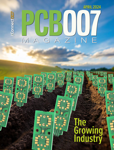
The Growing Industry
In this issue of PCB007 Magazine, we talk with leading economic experts, advocacy specialists in Washington, D.C., and PCB company leadership to get a well-rounded picture of what’s happening in the industry today. Don’t miss it.

The Sustainability Issue
Sustainability is one of the most widely used terms in business today, especially for electronics and manufacturing but what does it mean to you? We explore the environmental, business, and economic impacts.

The Fabricator’s Guide to IPC APEX EXPO
This issue previews many of the important events taking place at this year's show and highlights some changes and opportunities. So, buckle up. We are counting down to IPC APEX EXPO 2024.
- Articles
Article Highlights
- Columns
Search Console
- Links
- Events
||| MENU - pcb007 Magazine
AltiumLive Munich: Day 2 Keynotes
January 29, 2019 | Pete Starkey, I-Connect007Estimated reading time: 12 minutes
Having enjoyed the conference dinner and robot battles of the previous evening, a good night’s sleep, and a hearty breakfast, Altium’s family of over 220 electronics engineers and designers eagerly returned to the conference room. Many jostled to secure the best seats for the second day of the European AltiumLive design summit in Munich, keen to make the most of the “learn, connect, and get inspired” opportunity it offered.
Surprise!
Judy Warner, Altium’s director of community engagement, welcomed everyone and began the morning’s proceedings with a surprise item not published in the agenda, showing an example of Altium’s policy of supporting startup companies. She introduced Nikita Rodichenko, CTO of Tsuru Robotics. His company was founded in 2015 in Moscow. Currently, a team of 13 people are engaged in full-cycle R&D on robotic designs and specialising in designing and building unmanned aerial vehicles—effectively aerial robots. From tiny drones for drone shows to larger drones for security and surveillance and huge drones capable of carrying a 50-kilogram payload, Tsuru had been working with Altium to produce the first drone-reference design for Altium Designer.
The objective was to create a smart, compact design, which was modular and scalable, accessible to developers, supported open-source software, and had computer-vision capabilities. Tsuru has been a beta user of Altium Designer 19 since June 2018 and had utilised Altium Design Workspaces to enable a group of mechanical and PCB engineers and designers to work collaboratively on the project together with Altium’s cooperation in supporting component and footprint information. Extensive use had been made of rigid-flex PCB designs to mitigate vibrational problems. The project had been carried out on a tight timescale, and the product had worked the first time.
What was next? A famous graffiti artist was commissioned by a multinational soft-drinks corporation and collaborated with Tsuru Robotics to develop a fully programmable graffiti drone and paint a 50-metre advertising graphic on the side of a building in the centre of Kiev! Rodichenko showed a video of the graffiti being created, which was a nice illustration of an unconventional drone application.
Two Davids
Following this excellent example of real-life user-experience came a real-time demonstration of Altium Designer 19 PCB capabilities presented by Altium product marketing engineer David Haboud with his colleague, David Marrakchi, technical marketing manager, with Marrakchi’s laptop hooked up to the big screens.
After engaging the audience with deep-breathing exercises, Haboud stressed the importance of Altium communicating at the engineer level with their users to obtain the feedback needed to guide their programme of continuous improvement. They had learned that only 8% of users had no mechanical constraints, 83% designed multiboard systems, and 85% were responsible for their own libraries. The importance of library management functions was rated seven out of 10, the importance of routing functions rated eight out of 10, and the importance of performance nine out of 10.
Current AD19 functional development areas fell into four main groups: impedance solver and differential pair enhancements in the high-speed area; a new 3D kernel and rigid-flex support in the 3D multi-board area; friendly component move, follow mode, stacked microvia, and pushed trace glossing in the routing area; and faster part search, unified components panel, and faceted searching in the library management area.
Marrakchi demonstrated the features and enhancements of Designer 19 in response to prompts from Haboud and many questions from the audience. There were many new automated routines, and some interesting 3D functions including design rules for printed electronics where the layer order was built up from the bottom and dielectric was automatically placed at crossover points between successive conductor layers. The two Davids could have spent many hours answering specific questions and demonstrating the detailed operation of Designer 19, but time was limited, and the audience was encouraged to find out more by registering on Altium’s website for a series of live online or on-demand webinars.
The PCB Doctor
By popular request, the PCB doctor made a return visit to AltiumLive. Thomas Wischnack made it clear that he had not assumed that title himself; it had been bestowed upon him by Judy Warner as an appropriate designation recognising his expertise in curing PCB problems, especially those related to EMC. “Remember that the PCB doctor doesn’t help developers to cure PCBs; he helps the PCBs and cures the developers!”
Wischnack, senior expert for hardware development at Porsche Engineering, had compiled a list of the top-10 common design pitfalls of 2018 and reviewed them one by one beginning at the bottom and working upwards. Case grounding was the tenth pitfall, and his advice was not to make DC connections to ground, to avoid unpredictable ground loops and currents, and instead make RF connections with suitably chosen resistors and capacitors.
Number nine was to resist the temptation to copy and paste from other designs unless they were fully understood or risk a high probability of problems. Number eight was to rationalise the placement of connectors, ideally all on one edge, to avoid unpredictable cross-currents and unpredictable behaviour of filters. Number seven was to avoid the over-use of common-mode chokes, as the disadvantages generally outweighed the benefits. Number six was to understand the return path for signals clearly and avoid unnecessary alternative grounds.
Number five concerned the intelligent placement and routing of filters to ensure that they actually did something useful. Number four was to get the layer stackup right to enable impedance-matched routing—even if it made the PCB more expensive—and to seek the assistance of the PCB fabricator in defining the optimum stackup. Number three was to make sure that high-speed signals were routed with matched impedance to avoid EMC problems and to use common ground planes as reference planes in high-speed systems.
Number two was to avoid ground flooding, a hot topic, and one on which Wischnak held very strong views. Ground flooding resulted in unpredictable ground currents, reference for high-speed signals, reference for voltage sensitive applications, and filter behaviour, and gave the “foggy hills” effect in the EMC spectrum.
The switching voltage regulator was at the top of Wischnack’s list, which in his opinion, is the primary cause of EMC issues and could cause trouble up to 1 GHz. He listed the main design failures, which included switch nodes being too big, poor ground layout, unshielded inductors, and wrong filter applications. However, he believed that manufacturers had responded to user feedback and that the performance of newer parts was improved.
Page 1 of 2
Suggested Items
iNEMI Packaging Tech Topic Series: Role of EDA in Advanced Semiconductor Packaging
04/26/2024 | iNEMIAdvanced semiconductor packaging with heterogenous integration has made on-package integration of multiple chips a crucial part of finding alternatives to transistor scaling. Historically, EDA tools for front-end and back-end design have evolved separately; however, design complexity and the increased number of die-to-die or die-to-substrate interconnections has led to the need for EDA tools that can support integration of overall design planning, implementation, and system analysis in a single cockpit.
Cadence, TSMC Collaborate on Wide-Ranging Innovations to Transform System and Semiconductor Design
04/25/2024 | Cadence Design SystemsCadence Design Systems, Inc. and TSMC have extended their longstanding collaboration by announcing a broad range of innovative technology advancements to accelerate design, including developments ranging from 3D-IC and advanced process nodes to design IP and photonics.
Ansys, TSMC Enable a Multiphysics Platform for Optics and Photonics, Addressing Needs of AI, HPC Silicon Systems
04/25/2024 | PRNewswireAnsys announced a collaboration with TSMC on multiphysics software for TSMC's Compact Universal Photonic Engines (COUPE). COUPE is a cutting-edge Silicon Photonics (SiPh) integration system and Co-Packaged Optics platform that mitigates coupling loss while significantly accelerating chip-to-chip and machine-to-machine communication.
Siemens’ Breakthrough Veloce CS Transforms Emulation and Prototyping with Three Novel Products
04/24/2024 | Siemens Digital Industries SoftwareSiemens Digital Industries Software launched the Veloce™ CS hardware-assisted verification and validation system. In a first for the EDA (Electronic Design Automation) industry, Veloce CS incorporates hardware emulation, enterprise prototyping and software prototyping and is built on two highly advanced integrated circuits (ICs) – Siemens’ new, purpose-built Crystal accelerator chip for emulation and the AMD Versal™ Premium VP1902 FPGA adaptive SoC (System-on-a-chip) for enterprise and software prototyping.
Listen Up! The Intricacies of PCB Drilling Detailed in New Podcast Episode
04/25/2024 | I-Connect007In episode 5 of the podcast series, On the Line With: Designing for Reality, Nolan Johnson and Matt Stevenson continue down the manufacturing process, this time focusing on the post-lamination drilling process for PCBs. Matt and Nolan delve into the intricacies of the PCB drilling process, highlighting the importance of hole quality, drill parameters, and design optimization to ensure smooth manufacturing. The conversation covers topics such as drill bit sizes, aspect ratios, vias, challenges in drilling, and ways to enhance efficiency in the drilling department.


