-

- News
- Books
Featured Books
- pcb007 Magazine
Latest Issues
Current Issue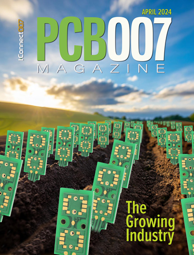
The Growing Industry
In this issue of PCB007 Magazine, we talk with leading economic experts, advocacy specialists in Washington, D.C., and PCB company leadership to get a well-rounded picture of what’s happening in the industry today. Don’t miss it.

The Sustainability Issue
Sustainability is one of the most widely used terms in business today, especially for electronics and manufacturing but what does it mean to you? We explore the environmental, business, and economic impacts.

The Fabricator’s Guide to IPC APEX EXPO
This issue previews many of the important events taking place at this year's show and highlights some changes and opportunities. So, buckle up. We are counting down to IPC APEX EXPO 2024.
- Articles
- Columns
Search Console
- Links
- Events
||| MENU - pcb007 Magazine
Chemical Recycling as Part of a Zero-effluent Strategy
March 6, 2019 | Happy Holden, I-Connect007Estimated reading time: 1 minute
Green manufacturing methodologies for PCBs are becoming a global shift. Green efforts have been underway in the European Union for quite some time. Likewise, in the United States, new PCB manufacturers are building zero-waste, zero-effluent facilities and gaining certification as such. Furthermore, in China, government mandates are transforming the amount of pollutants tolerated from PCB manufacturing down to nearly zero or face forced relocation from populated areas.
In this article, I will examine some of the key areas of improvement in chemical recycling that you should consider as you move your fabrication facility toward green and zero effluent manufacturing. For the scope of this article, I will use GreenSource Fabrication’s New Hampshire facility as our primary example.
New Example of Green for Printed Circuit Fabrication
To build a new PCB manufacturing facility in New Hampshire, GreenSource had to guarantee the government that they would be zero-effluent. While engineering the concepts of no effluents and being mindful of Six Sigma and Lean principles, the process is fully automated with minimal process delays and no handling by employees, thus being an excellent example of Lean plus green! The two go hand-in-hand.
The new facility does not require waste permits because there were no water emissions. Water is recycled, as are many of the chemicals, reducing costs. The totally automated process requires only seven technicians to monitor the machinery and a total of 17 staff people for the entire multilayer facility. As seen in Figure 1, the bulk of the PCB processing is conducted in numerous automated machines connected by conveyors or AGVs.
Figure 1: The main high-volume PCB processes are automated on several conveyorized systems from the materials warehouse (an automated storage and retrieval system, or AS/RS) through final solder mask and fabrication.
This article originally appeared in the January 2019 issue of PCB007 Magazine, click here.
Suggested Items
Taiyo Circuit Automation Installs New DP3500 into Fuba Printed Circuits, Tunisia
04/25/2024 | Taiyo Circuit AutomationTaiyo Circuit Automation is proud to be partnered with Fuba Printed Circuits, Tunisia part of the OneTech Group of companies, a leading printed circuit board manufacturer based out of Bizerte, Tunisia, on their first installation of Taiyo Circuit Automation DP3500 coater.
Vicor Power Orders Hentec Industries/RPS Automation Pulsar Solderability Testing System
04/24/2024 | Hentec Industries/RPS AutomationHentec Industries/RPS Automation, a leading manufacturer of selective soldering, lead tinning and solderability test equipment, is pleased to announce that Vicor Power has finalized the purchase of a Pulsar solderability testing system.
AIM Solder’s Dillon Zhu to Present on Ultraminiature Soldering at SMTA China East
04/22/2024 | AIMAIM Solder, a leading global manufacturer of solder assembly materials for the electronics industry, is pleased to announce that Dillon Zhu will present on the topic: Ultraminiature Soldering: Techniques, Technologies, and Standards at SMTA China East. This event is being held at the Shanghai World Expo Exhibition & Convention Center from April 24-25.
AIM to Highlight NC259FPA Ultrafine No Clean Solder Paste at SMTA Wisconsin Expo & Tech Forum
04/18/2024 | AIMAIM Solder, a leading global manufacturer of solder assembly materials for the electronics industry, is pleased to announce its participation in the upcoming SMTA Wisconsin Expo & Tech Forum taking place on May 7 at the Four Points by Sheraton | Milwaukee Airport, in Milwaukee, Wisconsin.
Hentec/RPS Publishes an Essential Guide to Selective Soldering Processing Tech Paper
04/17/2024 | Hentec Industries/RPS AutomationHentec Industries/RPS Automation, a leading manufacturer of selective soldering, lead tinning and solderability test equipment, announces that it has published a technical paper describing the critical process parameters that need to be optimized to ensure optimal results and guarantee the utmost in end-product quality.
