


 The Right Approach: I Hear the Train A Comin'
 It’s Only Common Sense: OCCAM—the Time Is Now
 Marcy's Musings: The Growing Industry
New High-speed 3D Surface Imaging Technology in Electronics Manufacturing Applications
October 9, 2019 | Juha Saily, Focalspec Inc.Estimated reading time: 2 minutes
Introduction
Line confocal sensors—and scanners based on them—are used in the imaging of surfaces, transparent materials, and multi-layered structures in various metrology and inspection applications on discrete parts, assemblies, webs, and other continuous products. Examples of well-suited applications for line confocal technology include glossy, mirror-like, transparent and multi-layered surfaces made of metals (connector pins, conductor traces, solder bumps, etc.), polymers (adhesives, enclosures, coatings, etc.), ceramics (components, substrates, etc.) and glass (display panels, etc.). Line confocal sensors operate at high speed and can be used to scan fast-moving surfaces in real-time as well as stationary product samples in the laboratory.
Imaging results can be used to characterize a product’s dimensions, form, surface topography, surface roughness, flatness, thickness, and 3D volume. The line confocal method also has a tomographic functionality, which enables the capture of 3D structures under transparent layers, as well as the simultaneous acquisition of 2D gray-scale (intensity) images from single or multiple surfaces with a large depth of focus covering the sensor’s entire Z range (up to 5.50 mm).
Line Confocal Method
Figure 1 shows the line confocal sensor models that are currently in production. Each sensor has two front lenses—one for its transmitter and another for the receiver.
Figure 2: Line confocal method principle.
Figure 2 depicts the sensor’s operating principle. The transmitter has a light source that emits white light containing all visible wavelengths. An optical assembly separates the light into wavelengths and focuses each color at a different distance from the sensor, forming a focal plane.
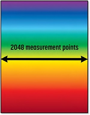
Depending on the vertical position of the imaged surface within the plane, corresponding wavelengths from 2,048 lateral points are reflected back to the sensor’s receiver. The receiver’s spectral camera captures wavelength and intensity information from each point to form related height and gray-scale profile lines. When the surface is moved in front of the sensor, a 3D point cloud and 2D grayscale image are generated from the scanned area line by line. The resulting data can be processed, analyzed, and reported with various 3D surface analysis and image processing software packages.
Line Confocal Method Imaging Capabilities
The line confocal sensors and systems work well in applications that require high-speed imaging of challenging materials at sub-micron resolution. Scanning an area that would require minutes or hours for traditional 3D imaging methods, such as point confocal or interferometric technologies, can be completed within a few seconds.
Transparent materials and products with highly reflective or mirror-like surfaces are ideal for the line confocal method. The sensors’ large numerical aperture and high tolerance for surface angle allow for imaging of steep slopes and glossy curved surfaces. This method does not suffer from speckle noise; this enables surface imaging at a much higher resolution than laser triangulation sensors.
The quality of the raw image data produced by the line confocal sensors is good and rarely needs filtering or other manipulation of any kind. Since the sensors capture 2,048 measurement points simultaneously, the vibration of the imaged surface or the sensor itself seldom causes issues; relative point height positions within the measurement profile line remain unaffected.
To read the full article, which appeared in the September 2019 issue of PCB007 Magazine, click here.
Share on:


Suggested Items
Taiyo Circuit Automation Installs New DP3500 into Fuba Printed Circuits, Tunisia
04/25/2024 | Taiyo Circuit AutomationTaiyo Circuit Automation is proud to be partnered with Fuba Printed Circuits, Tunisia part of the OneTech Group of companies, a leading printed circuit board manufacturer based out of Bizerte, Tunisia, on their first installation of Taiyo Circuit Automation DP3500 coater.
Vicor Power Orders Hentec Industries/RPS Automation Pulsar Solderability Testing System
04/24/2024 | Hentec Industries/RPS AutomationHentec Industries/RPS Automation, a leading manufacturer of selective soldering, lead tinning and solderability test equipment, is pleased to announce that Vicor Power has finalized the purchase of a Pulsar solderability testing system.
AIM Solder’s Dillon Zhu to Present on Ultraminiature Soldering at SMTA China East
04/22/2024 | AIMAIM Solder, a leading global manufacturer of solder assembly materials for the electronics industry, is pleased to announce that Dillon Zhu will present on the topic: Ultraminiature Soldering: Techniques, Technologies, and Standards at SMTA China East. This event is being held at the Shanghai World Expo Exhibition & Convention Center from April 24-25.
AIM to Highlight NC259FPA Ultrafine No Clean Solder Paste at SMTA Wisconsin Expo & Tech Forum
04/18/2024 | AIMAIM Solder, a leading global manufacturer of solder assembly materials for the electronics industry, is pleased to announce its participation in the upcoming SMTA Wisconsin Expo & Tech Forum taking place on May 7 at the Four Points by Sheraton | Milwaukee Airport, in Milwaukee, Wisconsin.
Hentec/RPS Publishes an Essential Guide to Selective Soldering Processing Tech Paper
04/17/2024 | Hentec Industries/RPS AutomationHentec Industries/RPS Automation, a leading manufacturer of selective soldering, lead tinning and solderability test equipment, announces that it has published a technical paper describing the critical process parameters that need to be optimized to ensure optimal results and guarantee the utmost in end-product quality.