


 The Right Approach: I Hear the Train A Comin'
 It’s Only Common Sense: OCCAM—the Time Is Now
 Marcy's Musings: The Growing Industry
Nano Dimension Sells Two DragonFly IV 3D-AME Systems to Defense and Government Agencies
December 6, 2021 | Nano Dimension Ltd.Estimated reading time: 2 minutes
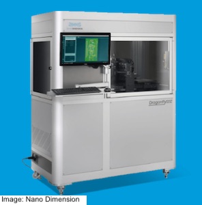
Nano Dimension Ltd., an industry-leader in Additively Manufactured Electronics (AME), Printed Electronics (PE), and Micro Additive Manufacturing (Micro-AM), announced that it has sold the first two DragonFly IV 3D-AME Printers, in addition to the two machines that have completed beta sites processes with other leading customers.
Nano Dimension is the leading provider of intelligent machines for the fabrication of AME. The new DragonFly IV system, combined with FLIGHT software, delivers new levels of quality, efficiency, and print resolution in the 3D printed electronics sector, providing increased flexibility to design any 3D geometry and create innovative new products.
DragonFly IV is a Dielectric and Conductive-Materials Additive Manufacturing System aimed for fabrication of High-Performance Electronic Devices (Hi-PEDs®) by depositing the proprietary materials simultaneously, while concurrently integrating in-situ capacitors, antennas, coils, transformers, and electro-mechanical components.
DragonFly IV 3D-AME Printer
DragonFly IV delivers improved accuracy of traces, spacing, and vias, improved PCB product quality, and the ability to design and produce 3D Hi-PEDs® in a one-step production process.
New capabilities include:
- Integration with Nano Dimension’s new FLIGHT software
- Integration of 3D elements in PCB
- 3D designed Hi-PEDs®
- Support of HDI level elements
- 75µm traces; 100µm spacing; 150µm via
- Enhanced print quality, optimizing yield with predictable conductivity
- Low thickness variation
FLIGHT Software Package
Nano Dimension’s new FLIGHT software suite provides a comprehensive first-of-a-kind ability to incorporate ECAD designs into real 3D MCAD designs, as well as intelligent verification, slicing, and job control solutions. FLIGHT enables the 3D design of electrical and mechanical features in 3-dimensions while ensuring that the new product designs comply with the system’s requirements and can then proceed directly to fabrication on the DragonFly IV.
The Flight Software Suite consists of 3 components:
1-FLIGHT Plan: Allows designers to develop viable 3D AME using both existing 2D design data, and novel 3D data. Tests show that this reduces the 3D AME design time by up to 10 times.
- Integrates 3D MCAD and ECAD capabilities for 3D Electro-Mechanical design
- Imports existing designs from major ECAD systems
- Enables the use of customers’ existing design tools
2-FLIGHT Check: This application enables design rule checks so that the designs meet the DragonFly IV requirements and are ready for printing.
- Unifies design rules for ECAD that meet the constraints of DragonFly IV
- Reduces design iteration cycles
3-FLIGHT Control: Delivers an entirely new pre-production solution that enables concurrent fabrication of both 2D and 3D multi-material Hi- PEDs®, improving productivity.
- Integrates system and job management toolsets
- Supports new file formats (STL & ODB++)
- Improves user experience through better rendering accuracy and user interface
Share on:


Suggested Items
iNEMI Packaging Tech Topic Series: Role of EDA in Advanced Semiconductor Packaging
04/26/2024 | iNEMIAdvanced semiconductor packaging with heterogenous integration has made on-package integration of multiple chips a crucial part of finding alternatives to transistor scaling. Historically, EDA tools for front-end and back-end design have evolved separately; however, design complexity and the increased number of die-to-die or die-to-substrate interconnections has led to the need for EDA tools that can support integration of overall design planning, implementation, and system analysis in a single cockpit.
Cadence, TSMC Collaborate on Wide-Ranging Innovations to Transform System and Semiconductor Design
04/25/2024 | Cadence Design SystemsCadence Design Systems, Inc. and TSMC have extended their longstanding collaboration by announcing a broad range of innovative technology advancements to accelerate design, including developments ranging from 3D-IC and advanced process nodes to design IP and photonics.
Ansys, TSMC Enable a Multiphysics Platform for Optics and Photonics, Addressing Needs of AI, HPC Silicon Systems
04/25/2024 | PRNewswireAnsys announced a collaboration with TSMC on multiphysics software for TSMC's Compact Universal Photonic Engines (COUPE). COUPE is a cutting-edge Silicon Photonics (SiPh) integration system and Co-Packaged Optics platform that mitigates coupling loss while significantly accelerating chip-to-chip and machine-to-machine communication.
Siemens’ Breakthrough Veloce CS Transforms Emulation and Prototyping with Three Novel Products
04/24/2024 | Siemens Digital Industries SoftwareSiemens Digital Industries Software launched the Veloce™ CS hardware-assisted verification and validation system. In a first for the EDA (Electronic Design Automation) industry, Veloce CS incorporates hardware emulation, enterprise prototyping and software prototyping and is built on two highly advanced integrated circuits (ICs) – Siemens’ new, purpose-built Crystal accelerator chip for emulation and the AMD Versal™ Premium VP1902 FPGA adaptive SoC (System-on-a-chip) for enterprise and software prototyping.
Listen Up! The Intricacies of PCB Drilling Detailed in New Podcast Episode
04/25/2024 | I-Connect007In episode 5 of the podcast series, On the Line With: Designing for Reality, Nolan Johnson and Matt Stevenson continue down the manufacturing process, this time focusing on the post-lamination drilling process for PCBs. Matt and Nolan delve into the intricacies of the PCB drilling process, highlighting the importance of hole quality, drill parameters, and design optimization to ensure smooth manufacturing. The conversation covers topics such as drill bit sizes, aspect ratios, vias, challenges in drilling, and ways to enhance efficiency in the drilling department.