-

- News
- Books
Featured Books
- pcb007 Magazine
Latest Issues
Current Issue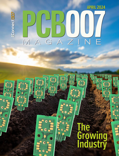
The Growing Industry
In this issue of PCB007 Magazine, we talk with leading economic experts, advocacy specialists in Washington, D.C., and PCB company leadership to get a well-rounded picture of what’s happening in the industry today. Don’t miss it.

The Sustainability Issue
Sustainability is one of the most widely used terms in business today, especially for electronics and manufacturing but what does it mean to you? We explore the environmental, business, and economic impacts.
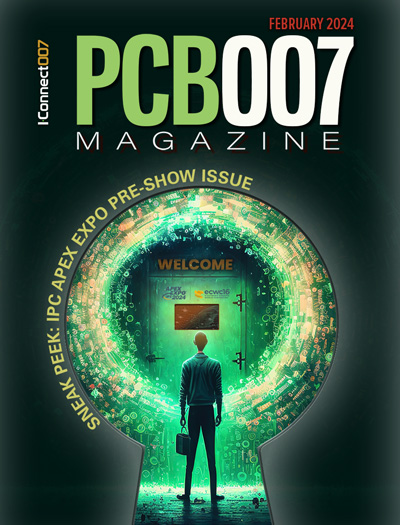
The Fabricator’s Guide to IPC APEX EXPO
This issue previews many of the important events taking place at this year's show and highlights some changes and opportunities. So, buckle up. We are counting down to IPC APEX EXPO 2024.
- Articles
Article Highlights
- Columns
Search Console
- Links
- Events
||| MENU - pcb007 Magazine
iNEMI Call-for-Participation Webinar: PCB Connector Footprint Tolerance Project
May 4, 2023 | iNEMIEstimated reading time: 1 minute
Size reduction coupled with increased bandwidth is driving new and tighter PCB/FPC (flexible printed circuit) design requirements that may exceed the capability of fabrication processes used for previous generations of I/O connector interfaces. In short, connector land pattern tolerances drive process requirements not previously needed. An understanding of complex process interactions is necessary to identify processes to use, conduct risk assessment, and meet product quality requirements.
The purpose of iNEMI’s PCB Connector Footprint Tolerance project is to define methods that enable designers who are creating products with high I/O bandwidth connector footprints to use the collected industry capability and capacity data to determine appropriate mitigation for the required level of quality for a given product. This fast-turnaround project will:
- Provide better understanding of risks associated with high I/O bandwidth connector footprints
- Enable product designers to conduct risk assessments to determine optimum manufacturing processes to enable PCB suppliers to meet product quality requirements
- Reduce product qualification costs and associated time to market
Registration
Join us for our call-for-participation webinar to learn more about this new project. Two sessions are scheduled and are open to industry; advance registration is required, visit iNEMI's website.
Session 1
Tuesday, May 9, 2023
11:00 am. — 12:00 p.m. EDT (US)
5:00-6:00 p.m. CEST (Europe)
Session 2
Wednesday, May 10, 2023
7:00-8:00 a.m. CST (China)
7:00-8:00 p.m. EDT (US) on May 9
Suggested Items
Koh Young Showcases Award-winning Inspection Solutions at SMTconnect with SmartRep in Hall 4A.225
04/25/2024 | Koh Young TechnologyKoh Young Technology, the industry leader in True 3D measurement-based inspection solutions, will showcase an array of award-winning inspection and measurement solutions at SMTconnect alongside its sales partner, SmartRep, in booth 4A.225 at NürnbergMesse from June 11-13, 2023. The following offers a glimpse into what Koh Young will present at the tradeshow:
Real Time with… IPC APEX EXPO 2024: Plasmatreat: Innovative Surface Preparation Solutions
04/25/2024 | Real Time with...IPC APEX EXPOIn this interview, Editor Nolan Johnson speaks with Hardev Grewal, CEO and president of Plasmatreat, a developer of atmospheric plasma solutions. Plasmatreat uses clean compressed air and electricity to create plasma, offering environmentally friendly methods for surface preparation. Their technology measures plasma density for process optimization and can remove organic micro-contamination. Nolan and Hardev also discuss REDOX-Tool, a new technology for removing metal oxides.
KYZEN to Promote Pair of Stencil Cleaning Chemistries at SMTA Ciudad Jaurez Expo & Tech Forum
04/25/2024 | KYZEN'KYZEN, the global leader in innovative environmentally friendly cleaning chemistries, will exhibit at the SMTA Ciudad Juarez Expo & Tech Forum, scheduled to take place Thursday, May 9, 2024 at the Injectronic Convention Center in Ciudad Jaurez, Chihuahua, Mexico. During the event the KYZEN Clean Team will focus on understencil cleaning products KYZEN E5631J and CYBERSOLV C8882.
Cadence, TSMC Collaborate on Wide-Ranging Innovations to Transform System and Semiconductor Design
04/25/2024 | Cadence Design SystemsCadence Design Systems, Inc. and TSMC have extended their longstanding collaboration by announcing a broad range of innovative technology advancements to accelerate design, including developments ranging from 3D-IC and advanced process nodes to design IP and photonics.
Listen Up! The Intricacies of PCB Drilling Detailed in New Podcast Episode
04/25/2024 | I-Connect007In episode 5 of the podcast series, On the Line With: Designing for Reality, Nolan Johnson and Matt Stevenson continue down the manufacturing process, this time focusing on the post-lamination drilling process for PCBs. Matt and Nolan delve into the intricacies of the PCB drilling process, highlighting the importance of hole quality, drill parameters, and design optimization to ensure smooth manufacturing. The conversation covers topics such as drill bit sizes, aspect ratios, vias, challenges in drilling, and ways to enhance efficiency in the drilling department.
