


 The Right Approach: I Hear the Train A Comin'
 It’s Only Common Sense: OCCAM—the Time Is Now
 Marcy's Musings: The Growing Industry
Rainbow Technology Systems to Launch Unique Singulation System at Productronica
October 12, 2015 | Rainbow Technology SystemsEstimated reading time: 2 minutes
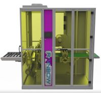
Rainbow Technology Systems, the company which brought the revolutionary Rainbow Process PCB production system to the electronics sector, is to introduce a unique Singulation System for use with digital imaging systems at this year’s Productronica exhibition.
The Rainbow Singulation System is a fully automated coating and laminating machine that takes a copper panel, cleans it, coats it both sides with solvent-free etch resist and laminates it with a thin layer of mylar. The edges of the panel are then sealed with UV light and panels are ejected ready for imaging in a digital imaging machine such as LDI or DMD.
Key to the process is Rainbow’s patented solvent-free etch resist which remains in a liquid state after coating. This removes the need for an oven as there is no solvent to release. The resist coating is thin ( <8 µm) and protected by mylar plus the machine automatically seals around the edge of each panel to offer easy, safe handling.
A key advantage of the system is that it will allow far faster throughput through a digital imaging machine as the Rainbow resist is much easier and faster to cure than dryfilm. After imaging, the mylar is peeled off and the panel goes through the develop, etch and strip stages in the same way as a dryfilm panel. As the thin coating and liquid state of the uncured resist allows faster developing, etching and stripping than normal it means the existing etch equipment can clear out higher density circuits (finer track and gap).
Jonathan Kennett, CEO, Rainbow Technology Systems said: “Our whole purpose at Rainbow is to find innovative ways of making the electronics production process easier, more efficient and more profitable. The new Singulation System achieves these aims for manufacturers using laser direct imaging equipment for PCB production.”
“We have spent many years to develop and refine the chemistry used in the solvent-free resist which is at the core of the cost and efficiency savings in the new system. This is the first significant change in the formulation of resist in the past 30 years so it is truly revolutionary, ” he added.
About Rainbow Technology Systems
The technology behind the Rainbow Singulation System is the brainchild of chief executive and founder Jonathan Kennett who set up Rainbow Technology Systems in 2005 to develop fine line printing technologies for the PCB market. Jonathan pioneered the development of contact cleaning technology for the electronics and high-tech sectors 25 years ago when he founded Teknek which has become the global leader in contact cleaning and yield improvement equipment. Other founder members of the senior management team include John Cunningham (chief chemist) and Robert Gibson (chief mechanical designer).
Share on:


Suggested Items
Designer’s Notebook: What Designers Need to Know About Manufacturing, Part 2
04/24/2024 | Vern Solberg -- Column: Designer's NotebookThe printed circuit board (PCB) is the primary base element for providing the interconnect platform for mounting and electrically joining electronic components. When assessing PCB design complexity, first consider the component area and board area ratio. If the surface area for the component interface is restricted, it may justify adopting multilayer or multilayer sequential buildup (SBU) PCB fabrication to enable a more efficient sub-surface circuit interconnect.
Insulectro’s 'Storekeepers' Extend Their Welcome to Technology Village at IPC APEX EXPO
04/03/2024 | InsulectroInsulectro, the largest distributor of materials for use in the manufacture of PCBs and printed electronics, welcomes attendees to its TECHNOLOGY VILLAGE during this year’s IPC APEX EXPO at the Anaheim Convention Center, April 9-11, 2024.
ENNOVI Introduces a New Flexible Circuit Production Process for Low Voltage Connectivity in EV Battery Cell Contacting Systems
04/03/2024 | PRNewswireENNOVI, a mobility electrification solutions partner, introduces a more advanced and sustainable way of producing flexible circuits for low voltage signals in electric vehicle (EV) battery cell contacting systems.
Heavy Copper PCBs: Bridging the Gap Between Design and Fabrication, Part 1
04/01/2024 | Yash Sutariya, Saturn Electronics ServicesThey call me Sparky. This is due to my talent for getting shocked by a variety of voltages and because I cannot seem to keep my hands out of power control cabinets. While I do not have the time to throw the knife switch to the off position, that doesn’t stop me from sticking screwdrivers into the fuse boxes. In all honesty, I’m lucky to be alive. Fortunately, I also have a talent for building high-voltage heavy copper circuit boards. Since this is where I spend most of my time, I can guide you through some potential design for manufacturability (DFM) hazards you may encounter with heavy copper design.
Trouble in Your Tank: Supporting IC Substrates and Advanced Packaging, Part 5
03/19/2024 | Michael Carano -- Column: Trouble in Your TankDirect metallization systems based on conductive graphite or carbon dispersion are quickly gaining acceptance worldwide. Indeed, the environmental and productivity gains one can achieve with these processes are outstanding. In today’s highly competitive and litigious environment, direct metallization reduces costs associated with compliance, waste treatment, and legal issues related to chemical exposure. What makes these processes leaders in the direct metallization space?