-

- News
- Books
Featured Books
- pcb007 Magazine
Latest Issues
Current Issue
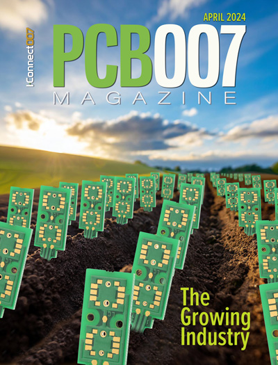
The Growing Industry
In this issue of PCB007 Magazine, we talk with leading economic experts, advocacy specialists in Washington, D.C., and PCB company leadership to get a well-rounded picture of what’s happening in the industry today. Don’t miss it.

The Sustainability Issue
Sustainability is one of the most widely used terms in business today, especially for electronics and manufacturing but what does it mean to you? We explore the environmental, business, and economic impacts.

The Fabricator’s Guide to IPC APEX EXPO
This issue previews many of the important events taking place at this year's show and highlights some changes and opportunities. So, buckle up. We are counting down to IPC APEX EXPO 2024.
- Articles
Article Highlights
- Columns
Search Console
- Links
- Events
||| MENU - pcb007 Magazine
Tim’s Takeaways: The Basics of Hybrid Design, Part 3
June 16, 2016 | Tim Haag, Intercept TechnologyEstimated reading time: 2 minutes
In the first two parts of this series, we discussed the basics of hybrid design from the PCB designer’s perspective, and this month we will conclude that discussion.
We are seeing more and more of our customers exploring the world of hybrid design, and we are getting new customers for whom hybrid design is their sole focus. The world of hybrid design is growing, and we have lots of hybrid-specific functionality built into our software that helps designers meet and conquer the unique hybrid design requirements that they are faced with.
And yet many designers out there (and I used to be one of them) have no idea what is meant when people start talking about hybrid design. It is therefore not uncommon for designers to avoid the subject directly while hoping to pick up little cues and pointers from others indirectly so that they are no longer in the dark. If that description sounds uncomfortably close to where you are at, then read on. My hope is that this three-part series will help you by serving as a basic introduction into the world of hybrid design.
If you haven’t had a chance to read the first two parts in this series, please go back to the last two months and take a look at them if you can. To summarize, however, we discussed in the first column the basic structure of hybrid designs and the benefits they offer over standard PCBs. In the second column we discussed some of the similarities and differences in CAD applications for the design of hybrids and how hybrid designs and their layer stackups are setup. We also discussed the routing of conductors (wires), and the creation of area fills and power planes. We continued from there talking about the creation of dielectric layers and their similarities and differences to fills and planes. Next we introduced the concept of cross-over dielectric layers, which is unique to hybrid designs, and how they are used. Finally we finished up with an explanation of how vias are created and managed in hybrids. Now, let’s talk about components.
The selection of components in a hybrid design is influenced by the operating temperature of the working design. Higher operating temperatures will require components that can withstand those extremes while at the same time necessitating a different amalgamation of soldering elements for manufacturing.
Passive components will use packaged parts while active components will use bare dies (no packaging). This is something different for the PCB designer who would rarely see a bare die used on a board design. Packaged active components can be used on a hybrid, but this is dependent upon the operating temperature of the design. And by using bare dies, a hybrid design realizes the benefits of shorter circuit paths, smaller size, and better thermal conditions for the device as it is glued directly to the substrate making for a better heat sink.
To read this entire article, which appeared in the May 2016 issue of The PCB Design Magazine, click here.
Suggested Items
Cadence, TSMC Collaborate on Wide-Ranging Innovations to Transform System and Semiconductor Design
04/25/2024 | Cadence Design SystemsCadence Design Systems, Inc. and TSMC have extended their longstanding collaboration by announcing a broad range of innovative technology advancements to accelerate design, including developments ranging from 3D-IC and advanced process nodes to design IP and photonics.
Ansys, TSMC Enable a Multiphysics Platform for Optics and Photonics, Addressing Needs of AI, HPC Silicon Systems
04/25/2024 | PRNewswireAnsys announced a collaboration with TSMC on multiphysics software for TSMC's Compact Universal Photonic Engines (COUPE). COUPE is a cutting-edge Silicon Photonics (SiPh) integration system and Co-Packaged Optics platform that mitigates coupling loss while significantly accelerating chip-to-chip and machine-to-machine communication.
Siemens’ Breakthrough Veloce CS Transforms Emulation and Prototyping with Three Novel Products
04/24/2024 | Siemens Digital Industries SoftwareSiemens Digital Industries Software launched the Veloce™ CS hardware-assisted verification and validation system. In a first for the EDA (Electronic Design Automation) industry, Veloce CS incorporates hardware emulation, enterprise prototyping and software prototyping and is built on two highly advanced integrated circuits (ICs) – Siemens’ new, purpose-built Crystal accelerator chip for emulation and the AMD Versal™ Premium VP1902 FPGA adaptive SoC (System-on-a-chip) for enterprise and software prototyping.
Listen Up! The Intricacies of PCB Drilling Detailed in New Podcast Episode
04/25/2024 | I-Connect007In episode 5 of the podcast series, On the Line With: Designing for Reality, Nolan Johnson and Matt Stevenson continue down the manufacturing process, this time focusing on the post-lamination drilling process for PCBs. Matt and Nolan delve into the intricacies of the PCB drilling process, highlighting the importance of hole quality, drill parameters, and design optimization to ensure smooth manufacturing. The conversation covers topics such as drill bit sizes, aspect ratios, vias, challenges in drilling, and ways to enhance efficiency in the drilling department.
Elevating PCB Design Engineering With IPC Programs
04/24/2024 | Cory Blaylock, IPCIn a monumental stride for the electronics manufacturing industry, IPC has successfully championed the recognition of the PCB Design Engineer as an official occupation by the U.S. Department of Labor (DOL). This pivotal achievement not only underscores the critical role of PCB design engineers within the technology landscape, but also marks the beginning of a transformative journey toward nurturing a robust, skilled workforce ready to propel our industry into the future.


