


 Happy’s Tech Talk #28: The Power Mesh Architecture for PCBs
 It’s Only Common Sense: Would You Join Your Own Company?
 The Chemical Connection: Reducing Etch System Water Usage, Part 2
MKS Introduces ESI Geode A CO2 Laser System for High Precision and High-Speed ABF IC Substrate Manufacturing
May 31, 2023 | MKS Instruments, Inc.Estimated reading time: 1 minute
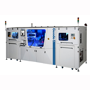
MKS Instruments, Inc., a global provider of technologies that transform our world, announced the official launch of the ESI Geode® A laser drill system today, a new configuration of the Geode® platform designed explicitly for drilling vias in the non-copper-clad ABF substrate market.
The Geode® A laser drilling system provides processing and application solutions for the FCBGA package substrate market, components which provide critical building blocks for everyday electronic devices and, in particular, high-performance computing. FCBGA substrates help enable supercomputing, artificial intelligence processing, autonomous cars, and other highly complex semiconductor modules.
“Manufacturers are under increased market pressure to deliver components that meet the precise demands of miniaturization and complexity required for advanced substrate manufacturing. At MKS, we are keenly focused on delivering the advanced technology needed for our customers to deliver next-generation productivity and quality,” said John Williams, MKS Vice President and General Manager of the ESI business. “In addition, the Geode® A laser drill is engineered as an integral component to the MKS Optimize the Interconnect SM solution, combining ESI laser drilling technologies with Atotech chemistry and plating equipment to provide customers with a full package of via formation technologies required to deliver optimal quality with the highest productivity for PCB and package substrate products.”
The Geode® A laser drilling system combines an innovative laser and optics configuration with precision pulse-shaping and beam-steering designed for ABF materials. These engineering innovations deliver the lowest cost of ownership and a greener manufacturing solution through 21% less floor space utilization, 72% less weight, and up to 65% less power consumption than the competition.
The Geode® A laser drilling system is available for purchase. More details can be found at www.esi.com, and system experts will be available at the JPCA 2023, Tokyo, Japan, May 31-June 2 in booth 6B-11.
Share on:


Suggested Items
The Chemical Connection: Reducing Etch System Water Usage, Part 2
05/02/2024 | Don Ball -- Column: The Chemical ConnectionIn my last column, I reviewed some relatively simple ways to reduce water usage in existing etch systems: cutting down cooling coil water flow, adding chillers to replace plant water for cooling, lowering flow rate nozzles for rinses, etc. This month, I’ll continue with more ways to control water usage in your etcher. Most of these are not easily retrofittable to existing equipment but should be given serious consideration when new equipment is contemplated. With the right combination of add-ons, it is possible to bring the amount of water used in an etch system to almost zero.
Designer’s Notebook: What Designers Need to Know About Manufacturing, Part 2
04/24/2024 | Vern Solberg -- Column: Designer's NotebookThe printed circuit board (PCB) is the primary base element for providing the interconnect platform for mounting and electrically joining electronic components. When assessing PCB design complexity, first consider the component area and board area ratio. If the surface area for the component interface is restricted, it may justify adopting multilayer or multilayer sequential buildup (SBU) PCB fabrication to enable a more efficient sub-surface circuit interconnect.
Insulectro’s 'Storekeepers' Extend Their Welcome to Technology Village at IPC APEX EXPO
04/03/2024 | InsulectroInsulectro, the largest distributor of materials for use in the manufacture of PCBs and printed electronics, welcomes attendees to its TECHNOLOGY VILLAGE during this year’s IPC APEX EXPO at the Anaheim Convention Center, April 9-11, 2024.
ENNOVI Introduces a New Flexible Circuit Production Process for Low Voltage Connectivity in EV Battery Cell Contacting Systems
04/03/2024 | PRNewswireENNOVI, a mobility electrification solutions partner, introduces a more advanced and sustainable way of producing flexible circuits for low voltage signals in electric vehicle (EV) battery cell contacting systems.
Heavy Copper PCBs: Bridging the Gap Between Design and Fabrication, Part 1
04/01/2024 | Yash Sutariya, Saturn Electronics ServicesThey call me Sparky. This is due to my talent for getting shocked by a variety of voltages and because I cannot seem to keep my hands out of power control cabinets. While I do not have the time to throw the knife switch to the off position, that doesn’t stop me from sticking screwdrivers into the fuse boxes. In all honesty, I’m lucky to be alive. Fortunately, I also have a talent for building high-voltage heavy copper circuit boards. Since this is where I spend most of my time, I can guide you through some potential design for manufacturability (DFM) hazards you may encounter with heavy copper design.