


 The Right Approach: I Hear the Train A Comin'
 It’s Only Common Sense: OCCAM—the Time Is Now
 Marcy's Musings: The Growing Industry
LPKF: Calculating the Savings Potential for Depaneling
April 14, 2021 | LPKFEstimated reading time: 3 minutes
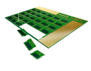
With the Panel Layout Optimization Tool (PLOT), LPKF offers a tool for calculating the materials savings that can be achieved with laser cutting.
In printed circuit board depaneling, laser technology users can achieve significant materials savings and thus considerably lower their costs with full-section cuts through the panels. This can be calculated with the new Panel Layout Optimization Tool (PLOT) from LPKF.
Promises of cost savings abound, but the extent to which they materialize is not always clear in advance – unless it is calculated using specific data. To make this possible, LPKF has developed a calculation tool that calculates the minimum material requirements for PCBs with laser full-section cutting and compares the results to those achieved with mechanical milling. It can be used on the company homepage simply and without any obligations. The user uploads the desired PCB layout and specifies the panel design. From these data, the PLOT calculates the materials savings and displays the result directly and clearly. An analysis document in PDF form is then made available to the user. The calculation runs via a secure server and meets the latest data protection standards.
Why Calculate?
Background for the development of the Panel Layout Optimization Tool: The right design for a panel is an extremely important factor in ensuring cost-efficient and low-error manufacturing of PCBs. If the panel area is used optimally, then more PCBs can be placed on one panel. This is advantageous with respect to both material usage and manufacturing efficiency.
However, the design process is subject to important guidelines and limitations, which are clearly presented on the LPKF website and in a white-paper available there. Challenges lie in the different geometries and component densities as well as in the need for technical cleanliness. The panel size and shape play a role as guidelines. A process-dependent border for handling is indispensable in some cases. These factors must be specified in the PLOT calculation tool from LPKF and are also used as the calculation basis. The calculation thus delivers a well-founded comparison of the utilization of panel sizes for milling and laser cutting.
Laser Technology Has an Advantage Here
Because the spacings between the PCBs and the cutting edge widths can be considerably smaller with a laser process than with mechanical depaneling processes, the material savings potential resulting from laser full-section cutting is very high. Premilled, relatively wide (2–3 mm) channels that are provided in mechanical depaneling processes and in routing for later cutting of tabs can be omitted in the panel design. Because laser processing provides a maximum amount of freedom in terms of geometry, the individual PCBs can be optimally placed and aligned on the panel. Overall materials savings of more than 30% on average, and even higher in some cases, can be achieved.
The maximized panel utilization also provides synergies in downstream process steps in PCB manufacturing because it significantly reduces handling requirements. The bigger the increase in panel utilization, the more significant the cost degression effects, especially for high lot volumes.
The next point chalked up on the laser side is the technical cleanliness, which leads to high-quality and reliable printed circuit boards. Milling dust is not an issue with laser cutting, and with LPKF CleanCut, there is no carbonization of the cut edges. Additionally, with laser cutting, mounting close to the cut edges is possible because there are virtually no mechanical stresses generated in the material in the regions around the cut edges. As a result, PCBs can be implemented more compactly – that’s another positive effect of using laser technology. In the end, there are a few arguments besides the lowered costs that speak in favor of the laser as the tool of choice for depaneling.
Share on:


Suggested Items
KIC’s Miles Moreau to Present Profiling Basics and Best Practices at SMTA Wisconsin Chapter PCBA Profile Workshop
01/25/2024 | KICKIC, a renowned pioneer in thermal process and temperature measurement solutions for electronics manufacturing, announces that Miles Moreau, General Manager, will be a featured speaker at the SMTA Wisconsin Chapter In-Person PCBA Profile Workshop.
The Drive Toward UHDI and Substrates
09/20/2023 | I-Connect007 Editorial TeamPanasonic’s Darren Hitchcock spoke with the I-Connect007 Editorial Team on the complexities of moving toward ultra HDI manufacturing. As we learn in this conversation, the number of shifting constraints relative to traditional PCB fabrication is quite large and can sometimes conflict with each other.
Standard Of Excellence: The Products of the Future
09/19/2023 | Anaya Vardya -- Column: Standard of ExcellenceIn my last column, I discussed cutting-edge innovations in printed circuit board technology, focusing on innovative trends in ultra HDI, embedded passives and components, green PCBs, and advanced substrate materials. This month, I’m following up with the products these new PCB technologies are destined for. Why do we need all these new technologies?
Experience ViTrox's State-of-the-Art Offerings at SMTA Guadalajara 2023 Presented by Sales Channel Partner—SMTo Engineering
09/18/2023 | ViTroxViTrox, which aims to be the world’s most trusted technology company, is excited to announce that our trusted Sales Channel Partner (SCP) in Mexico, SMTo Engineering, S.A. de C.V., will be participating in SMTA Guadalajara Expo & Tech Forum. They will be exhibiting in Booth #911 from the 25th to the 26th of October 2023, at the Expo Guadalajara in Jalisco, Mexico.
Intel Unveils Industry-Leading Glass Substrates to Meet Demand for More Powerful Compute
09/18/2023 | IntelIntel announced one of the industry’s first glass substrates for next-generation advanced packaging, planned for the latter part of this decade.